Download
1 / 35
430 likes | 762 Views
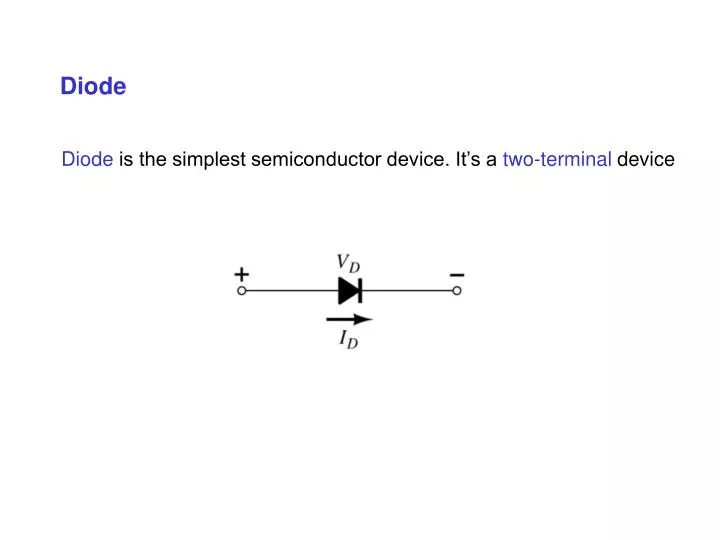
Diode. Diode is the simplest semiconductor device. It’s a two-terminal device. Basic operation. Ideal diode conducts current in only one direction and acts like open in the opposite direction. Characteristics of an ideal diode: Conduction region. Conduction region

E N D
Diode Diode is the simplest semiconductor device. It’s a two-terminal device
Basic operation Ideal diode conducts current in only one direction and acts like open in the opposite direction
Characteristics of an ideal diode: Conduction region Conduction region - the voltage across the diode is zero - the current near infinite - the diode acts like short
Characteristics of an ideal diode: Non-conduction region Www.cpe.kmutt.ac.th/~sanan Non-conduction region - all of the voltages is across the diode - the current is zero - the diode acts like open
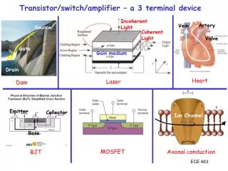
Semiconductor materials Two types of materials used in development of semiconductor are Silicon(Si) and Germanium(Ge) Doping is a process to add impurity(such as Antimony(Sb) or Boron(B)) to Si or Ge to make two types of semiconductor materials: n- type material: make Si(or Ge) more negative (has “free” electrons) p- type material: make Si(or Ge) more positive (has “holes”) Joining n-type and p-type materials makes a p-n junction diode
P-n junction diode “electrons” in n-types material migrate across the junction to p-type material and forms a so-called “depletion region” around the junction.
Resistance levels • DC or Static resistance • AC or Dynamic resistance • Average AC resistance
AC or Dynamic resistance Forward bias region: • The resistance depends on the amount of current(ID) in the diode. • The voltage across the diode is fairly constant(26 mA for 25 C). • rB ranges from a typical 0.1 Ohms for high power device to 2 Ohms for low power, general purpose diodes. Reverse bias region: • The resistance is infinite. The diode acts like an open.
Other types of diodes • Zener diode • Light emitting diode (LED) • Diode arrays
Diode equivalent circuits • Piecewise linear model • Simplified model • Ideal device
Determine VDQ, IDQ and VR if (a) E = 20 V, R = 1 kOhms (b) E = 10 V, R =10 kOhms
(a) E=20V, R = 1k: E = VD + VR = VD + RID Try VD = 0.5 = 19.5 mA = 19.5/1000 ID = (E - VD)/R From the graph, at ID = 19.5 mA, VD = 0.9 V Try VD = 0.9 = 19.1 mA = 19.1/1000 ID = (E - VD)/R Therefore, ID = 19.1 mA, VD = 0.9, VR = 19.1 V (b) E=10V, R = 10k: Try VD = 0.5 = 0.95 mA = 9.5/10000 ID = (E - VD)/R From the graph, at ID = 0.95 mA, VD = 0.55 V Try VD = 0.55 = 0.94 mA = 9.45/10000 ID = (E - VD)/R Therefore, ID = 0.94 mA, VD = 0.55, VR = 9.45 V
Example: Simple diode circuit Find VDQ, IDQ, and VR if (a) E = 10 Volts, R = 1 kOhms (b) E = 10 Volts, R = 2 kOhms (c) Repeat (a) using the approximate equivalent model for the Si diode. (d) Repeat (b) using the approximate equivalent model for the Si diode. (e) Repeat (a) using the ideal diode model. (f) Repeat (b) using the ideal diode model.
Example: (a) E = 10 Volts, R = 1 kOhms Y-intercept = E/R = 10 mA Slope = -1/ R = 1 mA/V From the load-line: IDQ = 9.15 mA VDQ = 0.82 V VR = IDQ x R = 9.15 V
Example: (b) E = 10 Volts, R = 2 kOhms Y-intercept = E/R = 5 mA Slope = -1/ R = 0.5 mA/V From the load-line: IDQ = 4.6 mA VDQ = 0.78 V VR = IDQ x R = 9.2 V