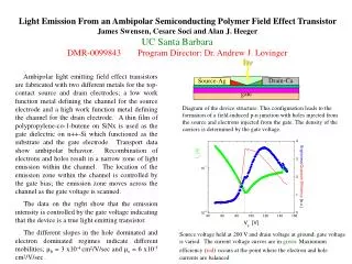
Download
1 / 17
170 likes | 422 Views
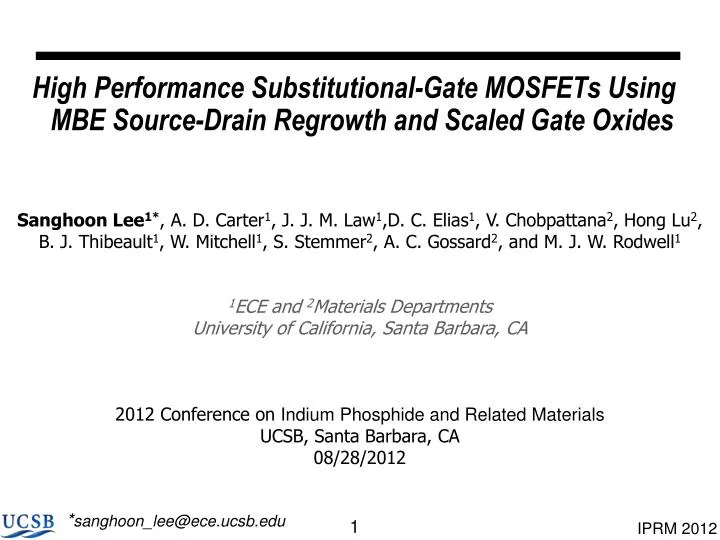
High Performance Substitutional-Gate MOSFETs Using MBE Source-Drain Regrowth and Scaled Gate Oxides. Sanghoon Lee 1* , A. D. Carter 1 , J. J. M. Law 1 ,D. C. Elias 1 , V. Chobpattana 2 , Hong Lu 2 , B. J. Thibeault 1 , W. Mitchell 1 , S. Stemmer 2 , A. C. Gossard 2 , and M. J. W. Rodwell 1

E N D
High Performance Substitutional-Gate MOSFETs Using MBE Source-Drain Regrowth and Scaled Gate Oxides Sanghoon Lee1*, A. D. Carter1, J. J. M. Law1,D. C. Elias1, V. Chobpattana2, Hong Lu2, B. J. Thibeault1, W. Mitchell1, S. Stemmer2, A. C. Gossard2, and M. J. W. Rodwell1 1ECE and 2Materials Departments University of California, Santa Barbara, CA 2012 Conference on Indium Phosphide and Related Materials UCSB, Santa Barbara, CA 08/28/2012 *sanghoon_lee@ece.ucsb.edu
Outline • Motivation: Why III-V MOSFETs? • Key Design Considerations • - Process : Gate-last • - Channel Design : Composite channel • - Gate dielectric • Process Flow • Measurement Results • - I-V Characteristics • - Gate leakage and TLM measurement • Conclusion
Why III-V MOSFETs in VLSI ? more transconductance per gate width more current→ speed or reduced Vdd → reduced power or reduced FET widths→ reduced IC size increased transconductance from: low mass→ high velocities lower density of states→ less scattering higher mobility in N+ regions → lower access resistance Other advantages strong heterojunctions→ carrier confinement wide range of available materials epitaxy→ atomic layer control
Key Design Considerations Process: Scalability (~10 nm-Lg,<30 nm contact pitch) : self-aligned S/D, very low ρc2) Carrier supply: heavily doped N+ source region3) Shallow junction: regrown S/D3) or Trench-gate Channel Design: Thinner wavefunction depth: Thin channel, less pulse doping. More density of state: L-vally transport channel4) Higher injection velocity: high In-content channel 5) Gate Dielectric: Thinner EOT: scaled high-k dielectric Low Dit: surface passivation6), reduced damage process7) 1) M. Wistey et al. EMC 2009; 2) A. Baraskar et al. IPRM 2010 ; 3) U. Singisetti et at. EDL 2009 ; 4) M. Rodwell et at., DRC 2010 5) S. Lee et al. EDL 2012 (accepted); 6) A. Carter et at. APEX 2011; 7) G. Burek, et al, JVST 2011.
Process : Why Gate-Last process? Gate-First Fully self-aligned transistor at nm dimensions Process damage during gate stack definition Large ungated region: High pulse doing Large leakage current and Decrease Cdepth A. Carter et at., DRC 2011 Gate-Last Low-damage process: Thermal gate metal, No Plasma process after gate dielectric deposition Rapid turn-around rapid learning.
Channel Design: Composite Channel S. Lee et al. EDL 2012 Average In-content high → Source-to-channel hetero-barrier suppressed Mean depth of wave function → reduce surface scattering Lower bound state m* → higher injection velocity
Gate Dielectric : Dit Passivation “False inversion” A. Carter et al., APEX 2012 • Cyclic hydrogen plasma / TMA treatments before dielectric growth 50 cycle (~5 nm Al2O3) growth, 400oC anneal, Ni metallization A. Carter et al., APEX 2012
Gate Dielectric : Dielectric Scaling 3.3/1.5 nm Al2O3/HfO2 1.65 nm EOT 1.1/4.0 nm Al2O3/HfO2 1.15 nm EOT Using H2+TMA+H2 treatment and Al2O3/HfO2 bilayer ~40% Thinner EOT with similar dispersion Courtesy of Gift in Stemmer’s Group
Gate Dielectric : Calculation for Dielectric scaling 1.1/4.0 nm Al2O3/HfO2(Experimental) 1.15 nm EOT 3.3/1.5 nm Al2O3/HfO2(Control) 1.65 nm EOT Assuming Ballistic FETs in the limit of degenerate carrier concentrations. Given a 7.5 nm channel, reducing 1.65 nm to 1.15 nm EOT → ~25% increase in Id/Wg
Process Flow SiO2 SiO2 SiO2 SiO2 N+ S/D N+ S/D Channel Channel Channel Channel Barrier Barrier Barrier Barrier Substrate Substrate Substrate Substrate Planarize amorphous InAs on dummy gates Deposit SiO2 as a dummy gate Pattern Dummy gate Regrow source/drain Ti/Pd/Au Al2O3/HfO2 Ni Ni N+ S/D N+ S/D N+ S/D Channel Channel Channel Barrier Barrier Barrier Substrate Substrate Substrate Deposit S/D contacts Lift-off gate metal Strip dummy gate Deposit dielectric Aneal
Measurement : I-V Curves for 50 nm-Lg devices Control : 3.3 nm Al2O3 / 1.5 nm HfO2 (1.65 nm EOT), 50 nm-Lg (as drawn) Experimental : 1.1 nm Al2O3 / 4.0 nm HfO2 (1.15 nm EOT) , 50 nm-Lg (as drawn) 1.0 mS/µm at Vds = 0.5 V : ~40% increase in transconductance. 0.8 mA/um at Vgs-Vth =0.8 V and Vds=0.5V : ~25% increase in on-current.
Measurement : I-V Curves for 200 nm-Lg devices Control : 3.3 nm Al2O3 / 1.5 nm HfO2 (1.65 nm EOT) , 200 nm-Lg (as drawn) Experimental : 1.1 nm Al2O3 / 4.0 nm HfO2 (1.15 nm EOT), 200 nm-Lg (as drawn) ~130 mV/dec SS for 1.15 nm EOT device : Dit and back-barrier leakage
Measurement : Gate leakage and TLM measurement Smaller gate leakage in 1.15 nm EOT device : slightly thick For both cases, gate leakage <10 nA/µm at all bias range ~1.0 Ohm-µm2 metal-semiconductor contact resistivity ~20 Ohm of sheet resistance
Conclusion • Developed Gate-last MOSFETs using MBE S/D regrowth • Decreasing EOT gives better performance with lower leakage • gm = ~ 1.0 mS/μm at Vds=0.5 V for a 50 nm-Lg device • Jd = 0.8 mA/μm at Vgs-Vth =0.8 V and Vds=0.5 V • for a 50 nm-Lg device • Future work: Thinner dielectric, Dit passivation, • and S/D leakage current
Thanks for your attention!Questions? This research was supported by the SRC Non-classical CMOS Research Center (Task 1437.006). A portion of this work was done in the UCSB nanofabrication facility, part of NSF funded NNIN network and MRL Central Facilities supported by the MRSEC Program of the NSF under award No. MR05-20415. *sanghoon_lee@ece.ucsb.edu
Device Physics : Ballistic transport In the limit of degenerate carrier concentrations ( Here, K is a function of m*, channel and dielectric thickness, and Dit ) Cdep Cdos Cox Injection velocity CDit Density of state capacitance Ef Ns Ewell 2DEG electron density Surface potential Wavefunction depth C Efermi-Ewell#1