Download
1 / 14
150 likes | 299 Views
High Transconductance Surface Channel In 0.53 Ga 0.47 As MOSFETs Using MBE Source-Drain Regrowth and Surface Digital Etching.

E N D
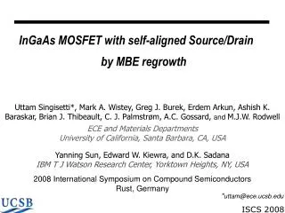
High Transconductance Surface Channel In0.53Ga0.47As MOSFETs Using MBE Source-Drain Regrowth and Surface Digital Etching Sanghoon Lee1*, C.-Y. Huang1, A. D. Carter1, J. J. M. Law1, D. C. Elias1, V. Chobpattana2, B. J. Thibeault1, W. Mitchell1, S. Stemmer2, A. C. Gossard2, and M. J. W. Rodwell1 1ECE and 2Materials Departments University of California, Santa Barbara, CA 2013 Conference on Indium Phosphide and Related Materials Kobe, Japan 05/22/2013 *sanghoon_lee@ece.ucsb.edu
Outline • Motivation: Why III-V MOSFETs? • Key Design Considerations • - Device Structure : Gate-last with S/D regrowth • - Damage during regrowth : surface digital etching • Process Flow • Measurement Results • - I-V Characteristics • - TLM measurement • Conclusion
Why III-V MOSFETs in VLSI ? more transconductance per gate width more current (at a fixed Vdd )→ IC speed or reduced Vdd (at a constant Ion)→ reduced power or reduced FET widths→ reduced IC size increased transconductance from: low mass→ high injection velocities lower density of states→ less scattering higher mobility in N+ regions → lower access resistance Other advantages heterojunctions→ strong carrier confinement wide range of available materials epitaxial growth→ atomic layer control
Key Design Considerations Device structure: Scalability (sub 20 nm-Lg,<30 nm contact pitch) : self-aligned S/D, very low ρc2) Carrier supply: heavily doped N+ source region3) Shallow junction: regrown S/D3) or Trench-gate Channel Design: Thinner wavefunction depth: Thin channel, less pulse doping. More injection velocity: high In-content channel4) Gate Dielectric: Thinner EOT : scaled high-k dielectric Low Dit : surface passivation5), minimized process damage6) 1) M. Wistey et al. EMC 2009; 2) A. Baraskar et al. IPRM 2010 ; 3) U. Singisetti et at. EDL 2009 ; 4) S. Lee et al. EDL 2012 (accepted); 5) A. Carter et at. APEX 2011; 6) G. Burek, et al, JVST 2011.
Device Structure : Gate-Last process Gate-First Fully self-aligned transistor at nm dimensions Process damage during gate metal deposition and definition Large ungated region: High pulse doing Large leakage current and increase in wavefunction depth A. Carter et at., DRC 2011 Gate-Last (substitutional-gate) Low-damage process: Thermal gate metal, No plasma process after gate dielectric deposition Rapid turn-around rapid learning.
Evidence of Surface Damage During Regrowth Long-channel FETs: consistently show >100 mV/dec. subthreshold swingIndicates high Dit despite good MOSCAP data. Suggests process damage. Experiment: SiO2 capping + high temp anneal + strip MOSCAP Process Finding: large degradation in MOSCAP dispersion. Confirms process damage hypothesis. Large dispersion Large Dit
Post-Regrowth Surface Digital Etching for Damage Removal - Surface removed by digital etch process2’ in BOE (dummy gate removal) , # cycles: 15’ UV ozone (surface oxidation) 1’ dilute HCl (native oxide removal) 13 - 15 Ȧ/cycle, ~0.16 nm RMS roughness - Etch significantly improves subthreshold swing and gm - Using this technique, we can easily thin the channel thickness.
Process Flow - Epitaxial layer growth - Dummy gate definition - InAs Source/Drain regrowth - Mesa isolation - InAs debris wet-etching - Dummy gate removal - Capping layer digital etching - S/D metal deposition - High-k deposition - Annealing - Gate metal deposition
I-V Characteristics for short and long channel devices - 1.6 mS/μm at Vds=0.5 V for a 65 nm-Lg device. - 95 mV/dec SS for a 530 nm-Lg device.
Comparison with a control sample (short channel) Control : without capping layer and surface digital etching, 75 nm-Lg Experimental : with surface digital etching , 75 nm-Lg - ~75 % increase in peak transconductance at Vds = 0.5 V - significantly better short channel characteristic with surface digital etching
Comparison with a control sample (long channel) Control : without surface digital etching, 500 nm-Lg Experimental : with surface digital etching, 535 nm-Lg - Similar on-state characteristics (~0.4 V Vt shift) - Better short channel effect
TLM Measurement for S/D metal contact - 0.15 ohm-μm2 Contact resistivity and 25 ohm/sq. sheet resistance. - 64 ohm-μm S/D access resistance (~5 % transconductance degradation)
Conclusion • Using digital etching, damaged surface can be effectively removed in a nanometer precision without etch-stop. • The removal of the damaged surface significantly improves both on- and off-state performance. • gm = 1.6 mS/μm at Vds=0.5 V for a 65 nm-Lg device • 95 mV/dec for a 530 nm-Lg device • InAs regrown S/D provides very low contact resistivity of 0.15 ohm-μm2 .
Thanks for your attention!Questions? This research was supported by the SRC Non-classical CMOS Research Center (Task 1437.006). A portion of this work was done in the UCSB nanofabrication facility, part of NSF funded NNIN network and MRL Central Facilities supported by the MRSEC Program of the NSF under award No. MR05-20415. *sanghoon_lee@ece.ucsb.edu