Download
1 / 47
540 likes | 997 Views
Microprocessor s 8255 PPI Programmable Peripheral I nterfac e. Outline. 8255 PPI 8255 PPI Pin Configuration 8255 operating modes 16-bit data bus to 8-bit peripherals MODE 0 Application (Keyboard) MODE 1 Application (Printer) MODE 2 Application (Printer). Pin Configuration.

E N D
Outline • 8255 PPI • 8255 PPI Pin Configuration • 8255 operating modes • 16-bit data bus to 8-bit peripherals • MODE 0 Application (Keyboard) • MODE 1 Application (Printer) • MODE 2 Application (Printer)
Pin Configuration • (CS)Chip Select. A “low’ on this input pin enables the communication between the 8255A, and the CPU. • (RD) Read. A “low” on this Input pin enables the 8255A to send the data or status information to the CPU on the data bus. In essence, it allows the CPU to “read from the 8255A. • (WR) Write. A. “ low” on the input pin enables the CPU to write data or control words into the 8255A. • (A0 and A1) Port Select 0 and Port Select 1. The Input signals, in conjunction with the RD and WR Inputs, controls the selection of one of the three ports or the control word registers. They are normally connected to the least significant bits of the address bus (A0 and A1).
Interface Registers A1 A0 RD WR CS Input Operation (Read) 0 0 0 1 0 Port A - Data Bus 0 1 0 1 0 Port B - Data Bus 1 0 0 1 0 Port C - Data Bus 1 1 0 1 0 Control Word - Data Bus Output Operation (Write) 0 0 1 0 0 Data Bus - Port A 0 1 1 0 0 Data Bus - Port B 1 0 1 0 0 Data Bus - Port C 1 1 1 0 0 Data Bus - Control
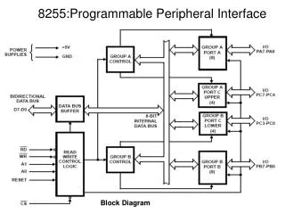
8255 A Block Diagram Showing Data Bus Buffer and Read/Write Control Logic Functions
Ports A, B and C • Ports A, B, and C The 8255A contains three 8-bit ports (A , B, and C). All can be configured in a wide variety of functional characteristics by the system software but each has its own special features or personally to further enhance the power and flexibility of the 8255A. • Port A. One 8 bit data output latch/buffer and one 8-bit data input latch. • Port B. One 8-bit data output latch/buffer and one 8-bit data input buffer. • Port C. One 8-bit data output latch/buffer and one 8-bit data input buffer (no latch for input). This port can be divided into two 4-bit ports under the mode control. Each 4-bit port contains a 4-bit latch and it can be used for the controls signal outputs and status signal inputs in conjunction with ports A and B.
8255A OPERATIONAL DESCRIPTION • Mode Selection There are three basic modes of operation that can be selected by the systems software: Mode O – Basic Input/Output Mode 1 – Strobed Input/Output Mode 2 – Bi-Directional Bus
16-bit data bus to 8-bit peripherals • The problem associated with connecting the 8-bit interface device to a 16-bit bus of an 8086 are releted to need to transfer even-addressed bytes over the lower half of the data bus and odd-addressed bytes over the upper half. BHE# A0 Transfer 0 0 Not useful 0 1 Odd addressed byte on upper half of bus 1 0 Even addressed byte on lower half of bus 1 1 Not possible
Solution 1: Use only even addresses • Example: We want to use a 8255 PPI with the starting I/O address of F8h. Use even adresses only. A7 A6 A5 A4 A3 A2 A1 A0 f8h 1 1 1 1 1 0 0 0 B : Port A fah 1 1 1 1 1 0 1 0 B : Port B fch 1 1 1 1 1 1 0 0 B : Port C feh 1 1 1 1 1 1 1 0 B : Control Reg. Register Select
Circuit Diagram D0-D7 8255 PPI CS RD# WR# A1 A0 D0-D7 A3 A4 A5 A0 0 1 2 3 4 5 6 7 A1 A2 From CPU ‘138 M/IO# A0 E1 E2 E3 A7 A6 IORDC# IOWRC# A2 A1
Access to Interface Registers • Port B and C are programmed as Mode 0 input port. • Port A is programmed as Mode 0 simple latched output port. • Write a code to implement the operation PortA=PortB-PortC mov AL,08Bh ;control word out 0FEh,AL ;written to control reg. in AL,0FCh ;Read Port C mov BL,AL ; in AL,OFAh ;Read Port B sub AL,BL ;PortB-PortC out 0F8h,AL ;write PortA
Solution 2: Use only odd addresses Example: We want to use a 8255 PPI with the starting I/O address of F9h. Use odd adresses only. A7 A6 A5 A4 A3 A2 A1 A0 f9h 1 1 1 1 1 0 0 1 B : Port A fbh 1 1 1 1 1 0 1 1 B : Port B fdh 1 1 1 1 1 1 0 1 B : Port C ffh 1 1 1 1 1 1 1 1 B : Control Reg. Register Select
Circuit Diagram D0-D7 8255 PPI CS RD# WR# A1 A0 D8-D15 A3 A4 A5 A0 0 1 2 3 4 5 6 7 A1 A2 From CPU ‘138 M/IO# E1 A0 E2 E3 A7 A6 IORDC# IOWRC# A2 A1
Solution 3: Use consecutive even and odd address Example: We want to use a 8255 PPI with the starting I/O address of C0h. Use even and odd adresses. A7 A6 A5 A4 A3 A2 A1 A0 C0h 1 1 0 0 0 0 0 0 B : Port A C1h 1 1 0 0 0 0 0 1 B : Port B C2h 1 1 0 0 0 0 1 0 B : Port C C3h 1 1 0 0 0 0 1 1 B : Control Reg. Register Select
D8-D15 74 245 OE# BHE# D0-D7 8255 PPI CS RD# WR# A1 A0 Y0 D0-D7 74 245 OE# A4 A3 A2 A0 0 1 2 3 4 5 6 7 A1 A2 From CPU ‘138 M/IO# A5 E1 E2 E3 A7 A6 IORDC# IOWRC# A1 A0
Example for BSR • Program 8255 for the following • A) set PC2 to high • B) Use PC6 to generate a square wave of 66% duty cycle • Solution • A) MOV AL, 00000101BOUT 92H,AL • B) AGAIN MOV AL, 0xxx1101OUT 92H, ALCALL DelayCALL DelayMOV AL, 0xxx1100OUT 92H, ALCALL DelayJMP AGAIN
Mode 0: Basic Input and Output This functional configuration provides simple input and output operations for each of the three ports. No ``handshaking'‘ is required, data is simply written to or read from a specified port. Mode 0 Basic Functional Definitions: • Two 8-bit ports and two 4-bit ports. • Any port can be input or output. • Outputs are latched. • Inputs are not latched. • 16 different Input/Output configurations are possible in this Mode.
MODE 0 Application (Keyboard Interface) • The switches in the keyboard are arranged in an array. The size of the array is described in terms of the number of rows and the number of the columns. • In our example, the keyboard array has four rows, which are labeled R0 through R3, and four columns, which are labeled C0 through C3. The location of the switch for any key in the array is uniquely defined by a row and a column. • For instance, the 0 key is located at the junction of R0 and C0, while the 1 key is located at R0 and C1. • In most applications, the microcomputer scans the keyboard array. That is, it strobes one row of the keyboard after the other by sending out a short-duration pulse, to the 0 logic level, on the row line. During each row strobe, all column lines are examined by reading them in parallel. • Typically, the column lines are pulled up to the 1 logic level; therefore, if a switch is closed, a logic 0 will be read on the corresponding column line. If no switches are closed, all 1s will be read when the lines are examined.
MODE 0 Application (Keyboard Interface) • The starting address for this I/O interface is 10H and consecutive even addresses are used. 10h: 0 0 0 1 0 0 0 0B -Port A (Output port) 12h: 0 0 0 1 0 0 1 0B -Port B (Unused output port) 14h: 0 0 0 1 0 1 0 0B -Port C (lower and higher input) 16h: 0 0 0 1 0 1 1 0B -Control Reg. PORTA EQU 10h PORTB EQU 12h PORTA EQU 14h CREG EQU 16h CWD EQU 10001001b MOV AL, CWD OUT CREG,AL
MODE 0 Application (Keyboard Interface) MATRIX DB ‘0123456789.+-x+*’ . . SCAN: MOV BL,0FEH ; send a short-duration pulse, to the 0 logic level, SCAN1: MOV AL,BL ; on the row line0. OUT PORTA,AL IN AL,PORTC ;Read PortC XOR AL,0FFH ;Complement AL AND AL,0FH ;Mask unused nibble CMP AL,0 JNE KEY ;if a key pressed go to KEY ROL BL,1 ; if no key pressed, shift the ruration pulse to next row CMP BL,0EFH JNE SCAN1 JMP SCAN . . KEY: . .
MODE 1 (Strobed Input/Output). This functional configuration provides a means for transferring I/O data to or from a specified port in conjunction with strobes or ``handshaking'' signals. In mode 1, Port A and Port B use the lines on Port C to generate or accept these ``handshaking'' signals. Mode 1 Basic functional Definitions: • Two Groups (Group A and Group B). • Each group contains one 8-bit data port and one 4-bit control/data port. • The 8-bit data port can be either input or output • Both inputs and outputs are latched. • The 4-bit port is used for control and status of the 8-bit data port.
Output Control Signal Definition OBF (Output Buffer Full F/F):The OBF output will go ``low'' to indicate that the CPU has written data out to the specified port. The OBF F/F will be set by the rising edge of the WR input and reset by ACK Input being low. ACK (Acknowledge Input): A ``low'' on this input informs the 82C55A that the data from Port A or Port B has been accepted. In essence, a response from the peripheral device indicating that it has received the data output by the CPU. INTR (Interrupt Request): A ``high'' on this output can be used to interrupt the CPU when an output device has accepted data transmitted by the CPU. INTR is set when ACK is a ``one'', OBF is a ``one'‘ and INTE is a ``one''. It is reset by the falling edge of WR. INTE A :Controlled by bit set/reset of PC6. INTE B: Controlled by bit set/reset of PC2.
Interrupt vs. Polling • CPU is interrupted whenever necessary • CPU can serve many devices • Require more hardware
Input Control Signal Definition STB (Strobe Input): A ``low'' on this input loads data into the input latch. IBF (Input Buffer Full F/F): A ``high'' on this output indicates that the data hasbeen loaded into the input latch; in essence, an acknowledgement. IBF is set by STB input being low and is reset by the rising edge of the RD input. INTR (Interrupt Request): A ``high'' on this output can be used to interrupt the CPU when an input device is requesting service. INTR is set by the STB is a ``one'', IBF is a ``one'‘ and INTE is a ``one''. It is reset by the falling edge of RD. This procedure allows an input device to request service from the CPU by simply strobing its data into the port. INTE A: Controlled by bit set/reset of PC4. INTE B: Controlled by bit set/reset of PC2.
Use of 8255 ports in PC MOV AL,99H OUT 63, AL