Download
1 / 36
1.06k likes | 2.6k Views
Peripheral Interface Device (8255 modes and examples). Dr A Sahu Dept of Computer Science & Engineering IIT Guwahati. Hierarchy of I/O Control Devices. 2 Port (A,B), No Bidirectional HS mode (C) 4 mode timer. 8155 I/O + Timer. 8255 I/O. 2 Port (A,B) A is Bidirectional

E N D
Peripheral Interface Device (8255 modes and examples) Dr A Sahu Dept of Computer Science & Engineering IIT Guwahati
Hierarchy of I/O Control Devices 2 Port (A,B), No Bidirectional HS mode (C) 4 mode timer 8155 I/O + Timer 8255 I/O 2 Port (A,B) A is Bidirectional HS mode (C) Extra controls 8253/54 Timer 6 mode timer 8259 Interrupt controller 8237 DMA controller 8251 Serial I/O USART controller
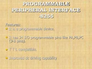
Outline • 8255 Architecture and its block diagram • 8255 Ports and mode of operations • BSR Mode • Mode 0 • Interfacing A/D Converter using Handshake mode using 8255 • Mode 1 • Interfacing DIP keyboard using Handshake mode using 8255 • Mode 2 • Interfacing keyboard (with bounce) using Handshake mode using 8255 • Introduction to interrupt controller (8259A)
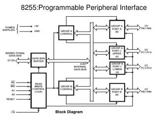
Block Diagram of 8255 Gr A Port A (8) I/O PA7-PA0 Group A Control I/O PC7-PC4 Gr A Port C (H 4) Bi directional Data Bus D7-D0 Data Bus Buffer Gr B Port C (L 4) I/O PC3-PC0 8 bit Internal Data Bus Read Write Control Logic RDb WRb A1 A0 RESET CSb Group B Control Gr B Port B (8) I/O PB7-PB0
Ports & Modes in 8255 8255 Port A D7 D6 D5 D4 D3 D2 D1 D CU Port C 0/1 CL Port B BSR Mode Bit Set/Reset I/O Mode BSR Mode Bit Set/Reset For Port C No Effect on I/O Mode Mode 0 Simple I/O for Ports A, B & C Mode 1 HS mode for Ports A and/or B Port C bits are used for HS Mode 2 Bidirectional Data mode for Port A B can in mode 0/1 Port C bits are used for HS
7 6 5 4 3 2 1 0 D7 D6 D5 D4 D3 D2 D1 D0 Group B Port C(L) – 1 Input 0 output Port B – 1 Input 0 output Mode select: 0 mode 0; 1 mode 1 Port C(U) – 1 Input 0 output Port A – 1 Input 0 output Mode select: 00 mode 0; 01 mode 1; 1x mode 2 1 – mode select 0 – bit set/reset Group A Ports & Modes in 8255 : Control register
I/O port Addressing CRW 83H 8255 A7 A6 A5 A4 A3 A2 Port A=80H CSb A1 A0 RDb WRb Port C=82H A1 A0 IORb IOWb Port B=81H Reset Reset
Group A Group B Port A Upper C Lower C Port B Ports • Control register controls the overall operation of 8255 • All three ports A, B and C are grouped into two
Operation modes • 8255 has three modes: - Mode 0: basic input-output - Mode 1: Strobbedinput-output - Mode 2: Strobbed bi-directinalbus I/O • In mode 0 - Two 8-bit ports and two 4-bit ports - Any port can be input or output - Outputs are latched, inputs are not latched
Operation modes • In mode 1: -Three ports are divided into two groups -Each group contains one 8-bit port and one 4-bit control/data port - 8-bit port can be either input or output and both latched - 4-bit port used for control and status of 8-bit data port • In mode 2 - Only port A is used - Port A becomes an 8-bit bidiectional bus - Port C acts as control port (only pins PC3-PC7 are used)
BSR (Bit Set or Reset Mode) • Set/Reset bit of Port C • Heavily used for HS and Interrupt mode • BSR Control word • BSR Control word • To set PC7= 0 000 111 1 (0FH) • To reset PC7= 0 000 111 0 (0EH) • To set PC3 = 0 000 011 1 (07H)
BSR Mode example • BSR Control word • To set PC7= 0 000 111 1 (0FH) • To reset PC7= 0 000 111 0 (0EH) • To set PC3 = 0 000 011 1 (07H) Generate Activation pulse of Delay D on PC7&PC3 MVI A,0FH ; Load ACC to set PC7 OUT 83H ; set PC7=1 MVI A,07H ; Load ACC to set PC3 OUT 83H ; set PC3=1 CALL DELAYD; MVI A,06H ; Load ACC to Reset PC3 OUT 83H ; set PC3=1 MVI A,0EH ; Load ACC to Reset PC7 OUT 83H ; set PC7=1
8255: Mode 0 • Simple I/O for port A,B,C • Output are latched • Input are not latched • Port don’t have HS or interrupt capability
8255: Mode 0, Example 1 • Configure • Port A and port CU as out port • Port B and port CL as in port • Interface to Read from I/P DIPs and Display at O/P LEDs • Control word 83H
Interface Circuit 8255 PA7 PA0 PC7 PC4 PC3 PC0 PB7 PB0 Buffer A7 A6 A5 A4 A3 A2 CRW 83H +5V 80H CSb A1 A0 RDb WRb Buffer 82H A1 A0 IORb IOWb 82H 81H Reset Reset +5V
Interface Program MVI A,83H ; Load acc with Control word OUT 83H ; Load control register with 83 at port address 83 IN 81H ; Read DIP from port B OUT 80H ; Write to LEDs IN 82H ; Read DIP from port C ANI 0FH ; Mask upper part of port C are not i/p RLC RLCRLCRLC; Rotate 4 time OUT 82H ; Display data at port CU HLT
8255: Mode 0, Example 2 • Air Conditioning Room (Temperature Control) • Heater and Cooler • Temperature Sensor • A/D converter • Driver Switch to drive Heater/Cooler • Design an A/C controller using 8255 and 8085 based interfacing circuit • Read temperature and control the temperature between 20-30 degree Celciuous
8255: Mode 0, Example 2 • Air Conditioning Room (Temperature Control) • Heater and Cooler • Temperature Sensor • A/D converter • Driver Switch to drive Heater/Cooler • Design an A/C controller using 8255 and 8085 based interfacing circuit • Read temperature and control the temperature between 20-30 degree Celsius • Use port A in mode 0 and Port C in BSR mode
Interface Circuit +5V 8255 PA7 PA0 PC0 PC4 PC7 PC5 PC6 ADC data LM135 Temp Sensor A7 A6 A5 A4 A3 A2 CRW 83H INTRb WRb RDb CSb A1 A0 RDb WRb A1 A0 IORb IOWb Cooler Relay Relay Heater Reset Reset + - 230V
Interface control • Control word • Port A as I/P from ADC • Port CL : as I/P PC0 is used for end of conversion • Port CU : as O/P PC4 -> Start con. PC7 ->assert RDb signal • BSR Control word • 0 (mode) 000 (don’t care) 000 (0/1=set/reset) • Set PC7 high = 0 000 111 1 = 0FH (Send RDb to ADC) • Set PC4 low = 0 000 100 0 = 08F (send Start ConvWRb) • Set PC5 high = 0 000 101 1 = 0BF (Fan On) • Set PC5 low = 0 000 101 0 = 0AF (Fan Off) 91H
Interface Program to do Temp. Control MVI A, 91H ; mode 0 control word OUT 83H ; Set A& CL as I/P & CU as O/P MVI A,0FH ;Set PC7 High OUT 83H ; Disable RDb MVI A,08H ; Set PC4 WRb low OUT 83H ; Start conversion MVI A, 09H ; Set PC4 WRb high OUT 83H ; Ser WRb high RD: IN 82H ; Read Port C to Chck PC0 RAR ; Place PC0 in Carry Flag JC RD ;if PC0=1, read Again MVI A,0EH ; Set PC7 RDb low OUT 83H ; Assert RDb signal IN 80H ; Read A/D conv. Port A MOV B,A ; get temp in B MVI A 0FH; ; Set PC7 (RDb) high OUT 83 ; Disable RDb MOV A,B; CPI 30D; CNC COOLEROFF; PC5 off 0AH CC COOLERON; PC5 on 0BH CPI 10D; MOV A,B; CNC HEATERON; PC6on: 0CH CC HEATEROFF; PC6off: 0DH RET COOLEROFF: MVI A, 0AH ; Reset PC5 to turn off Cooler OUT 83H RET
8255: Mode 1 • Two port A & V function 8 bit I/O • Configured either Input or output port • Each port each 3 lines of port C as HS signal • Remaining two lines can be used as simple I/O • Input and output are latched • Interrupt logic is supported PC6, PC7 in In/Out mode AEH
8255: Mode 1: Input Control signal • STBb: Strobe generated by Peripheral • IBF: Input buffer full • Acknowledge by 8255 to I/O that I/O latched received • Reset when MPU read the data • INTR: output signal to MPU and it generate when STBb=1, IBF=1 and INTE=1 • INTE: Enable or disable Interrupt • INTEA is through PC4, INTEB is through PC2 • Status word Mask with 02H
8255: Mode 1, Example • Designing for interfacing • Keyboard with interrupt I/O in port A • Output port for a printer using status check I/O • Control word • To generate interrupt INTEA PC4 to set in BSR mode • 0 (mode) 000 (don’t care) 000 (0/1=set/reset) • Set PC4 High = 0 000 100 1 = 09F (send INTR to MPU RST 6.5) B4H
Interface Circuit KBD 80A 8255 PA7 PA0 PC4 PC5 PC3 PC1 PC2 PB7 PB0 data A7 A6 A5 A4 A3 A2 CRW 83H STBb IBF CSb A1 A0 RDb WRb INTRA OBFb to PTR ACKb A1 A0 IORb IOWb 81H Printer Reset To RST 6.5
Interface Program Initialization Program MVI A, B4H ; initialize port A as IP and B as O/P OUT 83H MVI A,09H ; Set INTEA , that is PC4 EI ;Enable interrupt CALL PRINT ; Continue other Task ISR at 0034 at RST6.5 vector location 0034: JMP READPORTA READ PORTA: DI IN 80H MOV M, A INX H EI RET PRINT: LXI H MEM MVI B COUNT MOV A,M MOV C,A STATUS: IN 82H ; from port C for Status OBFb ANI 02H JNZ STATUS MOV A,C OUT 81H; Send to port B printer INX H DCR B JNZ NEXT RET
8255: Mode 2: Bi-directional Data transfer • Bi-directional • Data transfer between two MPU • Data transfer between MPU and Controller • Port A can be bi-directional, Port B in either 0 or 1 mode • Port A use 5 signals from port C as Handshake signal for data transfer
Bi-directional Data transfer between two MPU • One is Master other is Slave • Use 8255 as Interfacing device 8255 Master MPU Slave MPU OBFb PC7 PC6 PC5 PC4 PC3 ACKb Decode Logic CSb RDb WRb IBF STBb
Data Transfer From Mater to Slave • Master read the status of OBF to verify whether the previous byte has read by Slave • Mater write date in port A and 8255 inform to Slave by OBFb low • Slave check OBF for data availability • Slave read the data from port A and ACK low to 8255
Data Transfer From Slave to master • Slave check the HS signal IBF to find out whether port A is available or not • Slave Write a data in port A and inform 8255 by enabling STBb low • 8255 causes a IBF to go high and MPU get the signal the data byte to read • Master read the data from port A and make IBF low
Interface Circuit Slave MPU Master MPU 8255 PA7 PA0 PC7 PC5 PC6 PC4 data D7 D0 data A7 A6 A5 A4 A3 A2 CRW 83H CSb A1 A0 RDb WRb Latch TriState A1 A0 IORb IOWb A7 A6 A5 A2 A1 A0 EN IORb 3to8 Decoder ACKb 07 05 00 Reset STBb 80H=A 81H=B 82H=C 83H=CRW IORb 85H = A 87H = C IOWb
Control word Mode 2 • Control word • Status word: C0H Port C bit 2,1,0 mode 0/1 RAL instruction to get the Status
Interface program: Master & Slaves Master: LXI H, MemptrM MVI B, Byte2Trasfer MVI A, CTRL; Control word for Mode 2 OUT 83H; Write Control word OBFLO: IN 82H ; Read port C RAL ; place OBF in CY JNC OBFLO; OUT 80H ; place on Port A INX H DCR B JNZ OBFLO HLT SLAVE: LXI H, MemptrS MVI B, Byte2Trasfer OBFHI: IN 87H ; Read port C RAL ; place OBF in CY JC OBFHI; IN 85H ; Read from Port A MOV M, A INX H DCR B JNZ OBFHI HLT
Introduction to Interrupt controller8259A • Acts as a multiplexer, combining multiple interrupt input sources into a single interrupt output to interrupt a single device. • Original PC introduced in 1981 • Eight interrupt input request lines • IRQ0 - IRQ7, • An interrupt request output line named INTR • Interrupt acknowledgment line named INTA • D0 through D7 for communicating the interrupt level or vector offset. • There are three registers • Interrupt Mask Register (IMR) • Interrupt Request Register (IRR) • In-Service Register (ISR)
Reference • R S Gaonkar, “Microprocessor Architecture”, Chapter 15