Download
1 / 17
170 likes | 177 Views
Progress on resistive anodes and the large Prototype TPC. By: Stephen Turnbull. Outline. Why resistive films are necessary Resolution records broken just this last year A brief look at R&D Goals for the large prototype Bulk technologies

E N D
Progress on resistive anodes and the large Prototype TPC By: Stephen Turnbull
Outline • Why resistive films are necessary • Resolution records broken just this last year • A brief look at R&D Goals for the large prototype • Bulk technologies • Further work with the After chip developed for EUDET and used in T2K • Learning about photovoltaic techniques • Simulation work to predict desired properties • Next steps robustes,
Traditional spatial resolution limits • Traditional TPCs are limited in resolution by the Cluster width/pad width ratio. In short, only clusters E and F can be told apart from A,B,C,and D. • So with traditional TPC’s the options to improve resolution are • A. Increase Cluster sizes; • high Transverse diffusion gas • GEM stacks • Post amplification gas volume • B. or Decrease Pad Width; more channels.
Charge dispersion in a MPGD with a resistive anode • 2D Telegraph equation: • Modified MPGD anode with a high resistivity film bonded to a readout plane with an insulating spacer • Point charge at r = 0 & t = 0 disperses with time • The charge density r(r,t) at (r,t) is a solution of the 2D Telegraph equation • The anode charge density is time dependent and sampled by readout pads Q(t) (r) mesh resistive foil glue pads (r,t) integral over pads PCB M.S.Dixit et.al., NIM A518 (2004) 721 r (mm) t (ns)
Extrapolation of the ILC TPC Left: Micromegas with high Transverse diffusion gas( Analytical model). Best possible resolution in a very narrow window (150 – 350 mm) for 1mm pitch pads.Right, Black: Micromegas with Low diffusion gas, standard thin pads would be limited to a minimum of 130 resolution. Right Red: Micromegas with a resistive film and wide, 2.3 mm, pads. The ILC resolution goal can be achieved.
The Carleton chamber Carleton-Saclay Micromegas endplate with resistive anode. 128 pads (126 2mmx6mm in 7 rows plus 2 large trigger pads) Drift length: 15.7 cm ALEPH preamps + 200 MHz digitizers
The 5T cosmic-ray test at DESY 4 weeks of data taking (thanks to DESY and T. Behnke et al.) Used 2 gas mixtures: Ar+5% isobutane (easy gas, for reference) Ar+3% CF4+2% isobutane (so-called T2K gas, good trade-off for safety, velocity, large wt ) Most data taken at 5 T (highest field) and 0.5 T (low enough field to check the effect of diffusion) Note: same foil used since more than a year. Still works perfectly. Was ~2 weeks at T=55°C in the magnet: no damage
Resolution = 50 µ independent of the drift distance ‘T2K gas’ Resolution of 1/40th of pad width achieved! Results from these tests now published http://dx.doi.org/10.1016/j.nima.2007.07.099
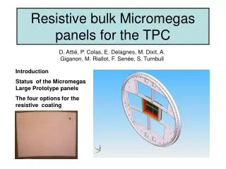
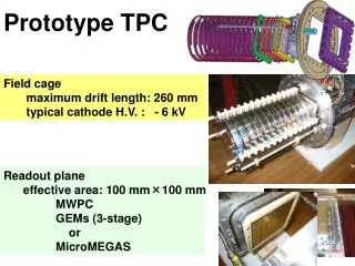
Our Next big goal Large Prototype panels f = 80cm Panels to be ready by the end of 2007, Cosmic tests to commence in January 2008 Beam tests starting summer 2008. All using AFTER Electronics Technology: Resistive Bulk Trigger : SiPM
Now add Resistive Functionality • Carleton-CERN-Orsay-Saclay… + others R&D collaboration towards a resistive ‘bulk’ Micromegas. • Options for the resistive anode: • Resistive paste (under test at CERN) • Resistive film (AlSi cermet) on mylar+glue • Thin film deposition on PCB or kapton or other (project at Neuchatel)
SCA: 76x511 Cells Front-end ASIC “AFTER” Technology: AMS CMOS 0.35mm Number of transistors: 400,000 Area: 7546mm x 7139 mm Package: LQFP 160 pins; 30 x 30 x 1.4 mm pitch: 0.65 mm Submission: 24 April 2006 Delivery: end of July 2006 Characterization: October 2006 – March 2007 Design features • 72 channels x 511 analog memory cells; Fwrite: 1-50 MHz; Fread: 20 MHz • 4 Charge Ranges (120 fC; 240 fC; 360 fC & 600 fC) • 16 Peaking Time Values (100 ns to 2 µs) – Or no shaping if desired. • MIP/noise: 100; I.N.L: 1% [0;3 Mips], 5% [3-10 Mips]
What we hope to do with Photovoltaic technologies • Deposits of resistive layers • Deposits of thin metal conductive pads • Learning about connections • LARGE surfaces at low Low LOW costs.
Simulation work yet still to come • Defining the relationship between the PRF and ultimate resolution. • Defining a new model for resistive pastes, rather then restive films sitting on a non-conducting glue
People I’ve stolen slides from • P. Colas • M. Dixit via D.Attie • D.Attie • M. Riallot (DAPNIA/SEDI) • D. P. Peterson • D. Calvet • And myself of course