Download
1 / 50
500 likes | 663 Views
The large prototype TPC A status report. Leif Jönsson Phys. Dept. Lund Univ. The field cage The end plate The infrastructure read-out electronics The TDC read-out. Goal: Develop a prototype TPC with all necessesary

E N D
The large prototype TPCA status report Leif Jönsson Phys. Dept. Lund Univ. The field cage The end plate The infrastructure read-out electronics The TDC read-out Goal: Develop a prototype TPC with all necessesary infrastructureto study the required performance of a full scale TPC for experiments at the ILC
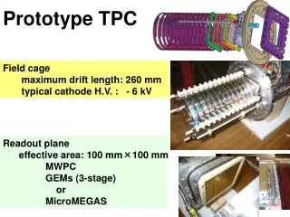
The field cage The size of the field cage is given by the dimensions of the magnet and the homogeneity of the magnetic field Length: 60 cm(the length over which the magnetic field strength vary by 1%) Radius: 40 cm( gives room for Si detectors between the coil and theTPC) Wall:composite material HV insulation:kapton layers Exchangable end-plate to test different gas amplification systems, cooling techniques, pad structures, mechanical stability, gas supply, gas tightness, HV distribution etc. Construction of the field cage in close collaboration with industry
Field maps - Width of field strips: 2.3 mm - Pitch: 2.8 mm Reduces the field inhomogeneities compared to 1.6 mm wide strips and 2.8 mm pitch (like in the present TPC prototype at DESY)
Field maps - Mirror strips at intermediate potentials - Kapton foil of 100 mm Very small field variations
Future plans • Beginning of 2007: construction of the field cage • Calculations to optimize the mechanical structure • Final design of field strips - Ongoing negotiations with industry concerning foils for the strips - Test samples of foils for electrical tests ordered
Example of signal routing from 1x4 mm2 pads to the WR-40S connector - Smalles foreseeable pad size 1x4 mm2 - The connector should match this size - Highest possible flexibility in pad geometry small modules - Japan Aviation Electronics offers a 40 pin connector with 0.5 mm pitch and dimensions 13.9x4.7 mm2 - 32 pins for signals and 8 pins for grounding
In case the front end card is connected via cables the arrangement may look the following way However the front end card can also connected directly onto the pad plane
The general test concept (as presented at NIKHEF) The intention is to build a modular electronic read-out system which offers a flexibility to test various types of avalanche read-out techniques and pad geometries. The read-out electronics should be dismountable from the pad board such that it can be easily moved from one panel to the next The amplifier board should be directly attached to the pad board via a connector The analogue and digital electronics should be mounted on separate cards connected by short ribbon cables The DAQ system should be flexible, such that it can be duplicated and distributed to different users performing table-top experiment. Is this still valid??? Option to test different types of amplifiers (shaping, non-shaping....)
17 cm 19 cm ALICE TPC Front End Card Integrated charge amplification, digitization and signal preprocessing in the TPC end plate 128 channels
Readout & Control Backplane Readout and Control Backplane 25 Front End Cards • Readout Bus (BW = 200 MB /sec) • VME-like protocol + syncrhonous block transfer • Control Bus (BW = 3 Mbit / sec) • I2C interface + interrupt feature • point-to-point lines for remote power control of FECs
USB to FEC Interface Card (U2F) The U2F Card can read up to 16 FECs (2048 channels) U2F Card
SPI Card + ALICE TPC FEC Temporary during the development phase of the new preamplifier Signal Polarity Inverter (SPI) Card
Status of the ALICE FEC 40-MHz ALTRO chip: about 125 chips have to be unsoldered from existing FECs (obsolete ALICE prototypes). This work is planned for Q1 2007. U2F and SPI cards: 2 additional boards of each type have been produced and tested New shaping amplifier chip: well advanced • - number of channels: 32 or 64 • - programmable charge amplifier: • sensitive to a charge in the range: ~102 - ~107 electrons • input capacitance: 0.1pF to 10pF
5 versions 7 standard channels Programmable Charge Amplifier INPUTS Production Engineering Data • 12- channel 4th order CSA • various architectures (classical folded cascode, novel rail-to-rail amplifier) • process: IBM CMOS 0.13 mm • area: 3 mm2 • 1.5 V single supply • Package: CQFP 144 • MPR samples (40): Apr ‘06 single channel OUTPUTS
Programmable Charge Amplifier • The CQFP 144 package has the same pin-count and similar pin-out as the ALICE TPC PASA • In the near future the new chip will be tested on a ALICE TPC FEC Next Step • Programmable Charge Amplifier (prototype) • 16 channel charge amplifier + anti-aliasing filter • Programmable peaking time (20ns – 140ns) and gain
System components and responsibilities • interface between TPC readout plane and FEE (Lund) • new shaping amplifer chip (CERN) • 40-MHz ALTRO (CERN) • Front End Card (PASA + ALTRO): • new design (Lund) • production and test (Lund) • U2F card (CERN) • System integration and test (Lund) • DAQ (Lund)
Pulse characteristics For tracks traversing the chamber parallel to the pad plane i.e perpendicular to the beam axis, the pulse length is determined by the longitudinal diffusion. For inclined tracks the pulse length is given by the difference in arrival time of the electrons emitted at the ends of the track segment covered by the length of a pad. Pulses will be of different length Options: Charge preamp, trise~40 ns, tdecay~2 ms and shaper integrator 200-500 ns 10 MHz sampling Charge preamp, trise~40 ns, tdecay 2 ~ms, no shaping, 25 MHz sampling Available:Charge preamp, trise 20-140 ns, shaping, 40 MHz sampling On discussion:The characteristics of the intrinsic GEM-pulse
Project Milestones Milestone I (Q1 2007) - Programmable Charge Amplifier (prototype); 16 channel charge amplifier + anti-aliasing filter Milestone II (Q2 2007) - 10-bit multi-rate ADC (prototype); 4-channel 10-bit 40-MHz ADC. The circuit can be operated as a 4-channel 40-MHz ADC or single-channel 160-MHz ADC.- Modified circuit board (design). Milestone III (Q3 2007) - Operating DAQ-system- Production and bench-top tests of modified FEC. Milestone IV (Q2 2008) - Charge Readout Chip (prototype); This circuit incorporates 32 (or 64) channels. -Mini FEC (design) Milestone V (Q4 2008) - Mini FEC (prototype) production and bench-top tests. Milestone VI (Q2 2009) ⇒ Charge Readout Chip (final version) - Production and final tests
Read-out using time-to digital converter Principle: Drift timemeasured by time-to-digital conversion Chargemeasured by charge-to-time conversion
The principle of the Amplifier Shaper Discriminator Q (charge)
Proof-of-principle experiments with GEM TPC at DESY Measurments with laser induced tracks. Calculated residuals for all hits. Resolution in Z: RMS ~0.4 mm (@ Z=30cm) 16 channel ASDQ board: preamplifier and charge-to-time converter A.Kaukher, "A study of readout electronics based on TDC for the international linear collider TPC detector", IEEE Trans. Nucl. Sci. 53 (2006) 749. First test: 128 channels EUDET (JRA2): 1000+ channel TDC-based compact readout electronics will be assembled.
Readout electronics for the LP TPC The readout electronics is (still) based on existing components: • Four 8-channel ASDQ ASIC (UPenn/FNAL) • 32-channel general puprose TDC (CERN) Small footprint of the board allows TPC pads as small as 1x4 mm2. Power consumption ~2 W/card ! 32 channel Front End Card(FEC): 4 ASDQ and HPTDC An “evaluation board” is being designed to investigate performance criteria to the analogue component – ASDQ, and the digital component – TDC, of the board. Next step: Front End Card (size :~30*100 mm2) A simple triple GEM detector is being prepared for standalone tests of the readout electronics. Next step: LP TPC
Read-out using time-to digital converter Principle: Drift timemeasured by time-to-digital conversion Chargemeasured by charge-to-time conversion
TDC-based readout electronics for a GEM TPC TDC-based FADC-based • The time of arrival is derived using the leading edge discriminator. • The charge of the input signal is encoded into the width of output digital pulse.
The mini-FEC new design • Motivation:should be compatible with the available area such that it can be mounted directly onto the connectors at the plane • the number of equipped pads can be increased without getting space problems.
Mini-FEC based on commercial components In telecommunication a completely new approach of handling signals has been developed (digitizing baseband + digital signal processing, DSP). Recent development in density and complexity of FPGA’s (field programmable gate array) and lower prices. Completely reprogrammable DSP in contrary to ASIC. A new generation of multi-channel, high-speed and high resolution FADC’s with low noise and serial digital output has been developed, offered to a reasonable cost.
Open questions What is the rise time of a typical GEM pulse? Mahdu Dixit claims around 100 ns or more Aachen measures around 40 ns with a 3 gap GEM structure and Ar/CH4 = 95/5 % • Shaping? • + the pulse shape is well-known • low sampling frequency enough • the integration time has to include • the longest possible pulse • loss in two-track resolution for shorter pulses No shaping? • + the sampling can be stopped at the • end of the pulse • best possible two-track resolution • the pulse shape is unknown or has to • be assumed to be known • needs higher sampling frequency?
Charge Readout Chip Block Diagram Anti-Aliasing Filter Anti-Aliasing Filter Anti-Aliasing Filter Signal Processor Signal Processor Signal Processor Data Compression Data Compression Data Compression Multi-Acq Memory Multi-Acq Memory Multi-Acq Memory Charge Amplifier Charge Amplifier Charge Amplifier ADC ADC ADC I N T E R F A C E Hit Finder • Maximize S/N • reduce quantization error • reduce signal bandwidth • Correct for crosstalk and common mode noise • Optimum pulse shaping for extraction of pulse features Feature Extaction Histogrammer 32 / 64 Channel
Starting point: min pad size 1 x 4 mm2 Requirements: highest possible flexibility in terms of pad geometry and shape of pad panels • Small modules (i.e. small connectors) Proposal: 32 channels modules, where each channel corresponds to an area of around 4 mm2 - Japan Aviation Electronics offers a 40 pin connector with 0.5 mm pitch and the dimensions 11.5 x 5 mm2. Thus, this connector allows additional 8 pins for grounding.
Readout electronics for the Large Prototype TPC (LPTPC) • modular with well defined interface for • various amplifcation technologies (GEM & µMegas) • different module geometries • easy to use and with a modern DAQ system • Two strategies pursued in EUDET • new TDC (Rostock) • FADC-based (Lund, CERN)
New development The programmable preamplifier • number of channels: 32 or 64 • programmable charge amplifier: • sensitive to a charge in the range: ~102- ~107 electrons • input capacitance: 0.1pF to 10pF
Field maps Mirror strips at intermediate potential No mirror strips Large field distortions (>5% at cathode Inhomogeneous field in drift region (O 1.5%) Small field variations (<0.5%) Some residue deviations at anode (O 1%) (needs optimizaton of inter- face end-plate drift volume)
Charge-to-time conversion in BELLE Lecroy MQT300A