Download
1 / 41
430 likes | 683 Views
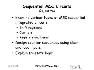
Sequential MSI Circuits Objectives. Examine various types of MSI sequential integrated circuits Shift registers Counters Registers and buses Design counter sequences using clear and load inputs Explain tri-state logic. 4-Bit Register. Q and Q’ both available Load on positive edge

E N D
Sequential MSI CircuitsObjectives • Examine various types of MSI sequential integrated circuits • Shift registers • Counters • Registers and buses • Design counter sequences using clear and load inputs • Explain tri-state logic ECEn 224 Winter 2002
4-Bit Register • Q and Q’ both available • Load on positive edge • Clear on CLR low ECEn 224 Winter 2002
6-Bit Register • Only Q available • Load on positive edge • Clear on CLR low • 6 bits instead of 4 • Still only 16 pins ECEn 224 Winter 2002
Integrated Shift Registers • Same basic function as the shift registers made of individual flip-flops • Different configurations available • Serial In, Parallel Out • Parallel In, Serial Out • Parallel In, Parallel Out with Shift • Universal Shift Register • Design tradeoffs • Number of bits, number of pins, number of functions ECEn 224 Winter 2002
8-Bit Shift Register • Serial in, parallel out • Shift on positive clock edge • Clear on CLR low • 14 pins ECEn 224 Winter 2002
8-Bit Shift Register • Parallel in, serial out • Select shift or load • Clear on CLR low • CLK and CLKINH for clocking • 16 pins ECEn 224 Winter 2002
4-Bit UniversalShift Register • Parallel in, parallel out • Shift right or left • Clear on CLR low • 16 pins ECEn 224 Winter 2002
4-Bit UniversalShift Register • Parallel in (load) • S1 = 1, S0 = 1 ECEn 224 Winter 2002
4-Bit UniversalShift Register • Shift Right • S1 = 0, S0 = 1 ECEn 224 Winter 2002
4-Bit UniversalShift Register • Shift Left • S1 = 1, S0 = 0 ECEn 224 Winter 2002
4-Bit UniversalShift Register • Hold (don’t shift) • S1 = 0, S0 = 0 ECEn 224 Winter 2002
4-Bit Ripple Counter • T flip-flops • Easy to construct • Not all counter outputs change at the same time to additional counter bits Clock Pulse ECEn 224 Winter 2002
4-Bit Ripple Counter 0 0 0 0 0 0 0 1 (0 0 0 0) 0 0 1 0 0 0 1 1 (0 0 1 0) (0 0 0 0) 0 1 0 0 . . . Clock Pulse ECEn 224 Winter 2002
4-Bit Ripple Counter . . . 1 1 1 1 (1 1 1 0) (1 1 0 0) (1 0 0 0) 0 0 0 0 Clock Pulse ECEn 224 Winter 2002
4-Bit SynchronousCounter • Parallel in • Count enable/disable • Clear on CLR low and CLK • 16 pins ECEn 224 Winter 2002
1 1 4-Bit SynchronousCounter • Count mode 1 0 0 1 0 0 0 (Orange is = 1) ECEn 224 Winter 2002
1 1 4-Bit SynchronousCounter • Count mode • RCO is ripple carry out = 1 when counter is 1111 1 0 0 1 0 0 0 (Orange is = 1) ECEn 224 Winter 2002
QA QB QC QD 4-Bit SynchronousCounter • Count not enabled 0 1 0 0 0 1 0 0 (Orange is = 1) ECEn 224 Winter 2002
4-Bit SynchronousCounter • Parallel load • Set LD_L to 0 (negative logic) • Apply inputs • Cycle the clock (0 to 1) • Load overrides count 1 1 1 1 0 0 1 1 (Orange is = 1) ECEn 224 Winter 2002
4-Bit SynchronousCounter • Clear • Set CLR_L to 0 (negative logic) • Cycle the clock (0 to 1) • Clear overrides load • (and count) 0 0 0 (Orange is = 1) ECEn 224 Winter 2002
4-Bit Synchronous Counter . . . ECEn 224 Winter 2002
4-Bit Synchronous Counter • Counter in continuous count mode ECEn 224 Winter 2002
4-Bit Synchronous Counter • Decade counter • Count 0 to 9, then to 0 • When counter output reaches 1001, reset overrides count ECEn 224 Winter 2002
4-Bit Synchronous Counter • Count from 7 (111) to 12 (1100) • Then cycle back to 7 • When counter output reaches 1100, load overrides count • Load of 0111 is forced ECEn 224 Winter 2002
4-Bit Synchronous Counter • More complex count sequences are possible • Normal: count in sequence • Use external gates to detect last value of sequential count • Use CLR if next count is 0 • Use LD if next count is non-0 • Use additional gates (if required) to set A, B, C, and D • See the book for more details ECEn 224 Winter 2002
4-Bit Synchronous Counter • Design for the count sequence 0000 to 0101 1010 to 1110 back to 0 ECEn 224 Winter 2002
4-Bit Synchronous Counter • Design for the count sequence 0000 to 0101 1010 to 1110 back to 0 ECEn 224 Winter 2002
4-Bit Synchronous Counter • Design for the count sequence 0000 to 0101 1010 to 1110 back to 0 Note the ‘problem” at 1101 ? ECEn 224 Winter 2002
4-Bit Synchronous Counter • Design for the count sequence 0000 to 0101 1010 to 1110 back to 0 • Use a Karnaugh map for more complex sequences ECEn 224 Winter 2002
8-Bit Synchronous Counter • Reset and load can still be used for count sequences other than straight binary • Just like the 4-bit counter • Larger counters can be built in a similar way ECEn 224 Winter 2002
3-State Logic • Used to transfer information back and forth between several registers • Used extensively in computer bus structures • Works sort of like a giant OR gate • Allows many gate outputs to be tied together ECEn 224 Winter 2002
3-State Logic ECEn 224 Winter 2002
3-State Logic • Outputs of 3-state buffers can be wired together • Only one buffer can be turned on at a time ECEn 224 Winter 2002
3-State Logic • 3-state (or tri-state) buffers are available with various inversions: ECEn 224 Winter 2002
8-Bit Register with Tri-State Outputs • Only Q available • Load on positive edge • Tie outputs to other tri-state outputs • No clear • 20 pins ECEn 224 Winter 2002
Register to Register Transfer • Design a circuit with four 8-bit registers • Use F1 F0 to specify the “from” register • Use T1 T0 to specify the “to” register • Use the LOAD pulse to transfer the data F1 F0 T1 T0 LOAD ECEn 224 Winter 2002
Wires named X1 through X8 Wide wire represents multiple wires Thin wire represents individual wires Connection to which bus wire is indicated A Word About Bus Notation ECEn 224 Winter 2002
Register to Register Transfer • Design a circuit with four 8-bit registers • Use F1 F0 to specify the “from” register • Use T1 T0 to specify the “to” register • Use the LOAD pulse to transfer the data F1 F0 T1 T0 LOAD ECEn 224 Winter 2002
Register to Register Transfer ECEn 224 Winter 2002
8-Bit Register with Tri-State Outputs • Only Q available • Load on positive edge • Tie outputs to other tri-state outputs • No clear • 20 pins ECEn 224 Winter 2002
Summary • Examine various types of MSI sequential integrated circuits • Shift registers • Counters • Registers and buses • Design counter sequences using clear and load inputs • Explain tri-state logic ECEn 224 Winter 2002