Download
1 / 5
50 likes | 199 Views
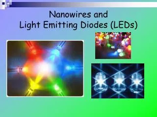
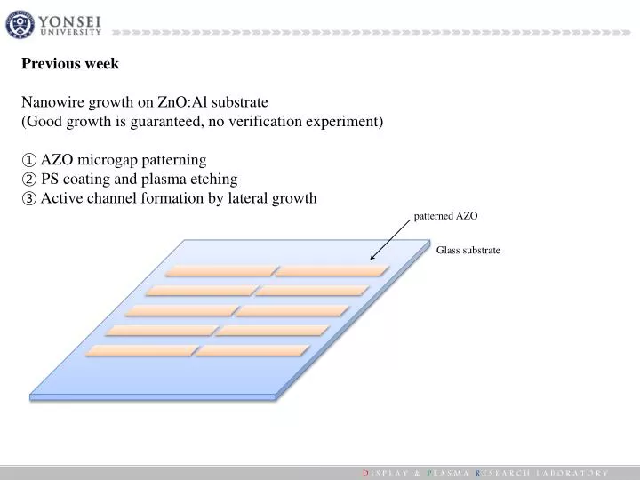
Previous week Nanowire growth on ZnO:Al substrate (Good growth is guaranteed, no verification experiment) ① AZO microgap patterning ② PS coating and plasma etching ③ Active channel formation by lateral growth . patterned AZO. Glass substrate. This week AZO etching

E N D
Previousweek Nanowire growth on ZnO:Al substrate (Good growth is guaranteed, no verification experiment) ① AZO microgap patterning ② PS coating and plasma etching ③ Active channel formation by lateral growth patterned AZO Glass substrate
Thisweek AZO etching Diluted HCl (ZnO etchant) didn’t work Etchant formula: HCl:HNO3:H2O = 4:1:500 ~330s is required for complete etching (~130s in ref.)
Thisweek Microgap patterning 1. Polystyrene etch mask (2000rpm 30s spin-coating, 150C baking) → did not endure acid etchant 2. PMMA etch mask (4000rpm 40s spin-coating, 175C baking) Razorblade is used for ~3um separation Following gap is widen and partially peeled off after etching Before etching After etching
Thisweek Microgap patterning Photolithography - 4000rpm 40s spin-coating - 90C 1min soft baking - 3min UV irradiation - 90C 1min hard baking ~10um gap is defined After AZO etching, PR is peeled off Suspection: Poor adhesion of photoresist Before etching After etching
Nextweek • Photoresist coating • HMDS treatment • Soft baking 110C 90s • Hard baking 130C 90s • ZnO lateral growth • PVP dielectric coating • Gate electrode coating • Device measurement

![Lecture 4: Factors affecting enzyme activity: [substrate] and inhibitors](https://cdn0.slideserve.com/394455/lecture-4-factors-affecting-enzyme-activity-substrate-and-inhibitors-dt.jpg)