Download
1 / 6
60 likes | 170 Views
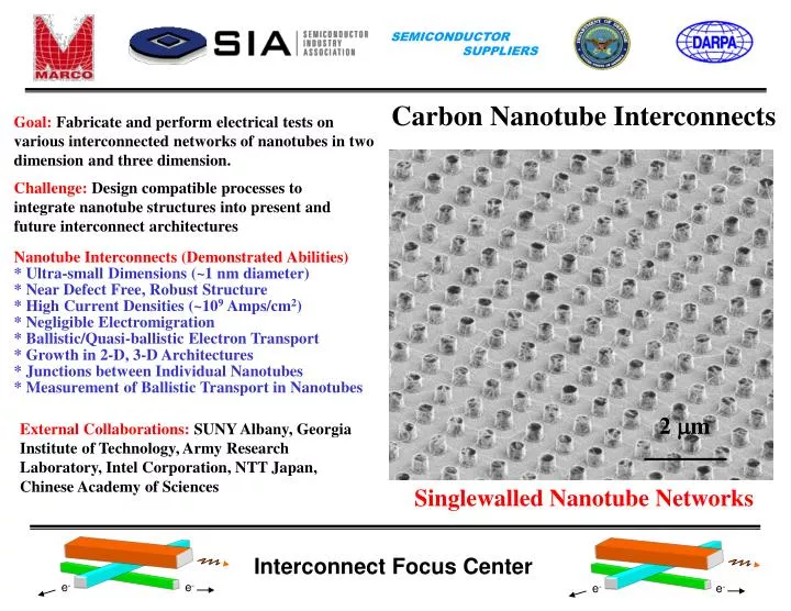
2 m m. Carbon Nanotube Interconnects. Goal: Fabricate and perform electrical tests on various interconnected networks of nanotubes in two dimension and three dimension. .

E N D
2 mm • Carbon Nanotube Interconnects Goal: Fabricate and perform electrical tests on various interconnected networks of nanotubes in two dimension and three dimension. Challenge: Design compatible processes to integrate nanotube structures into present and future interconnect architectures Nanotube Interconnects (Demonstrated Abilities) * Ultra-small Dimensions (~1 nm diameter) * Near Defect Free, Robust Structure * High Current Densities (~109 Amps/cm2) * Negligible Electromigration * Ballistic/Quasi-ballistic Electron Transport * Growth in 2-D, 3-D Architectures * Junctions between Individual Nanotubes * Measurement of Ballistic Transport in Nanotubes External Collaborations: SUNY Albany, Georgia Institute of Technology, Army Research Laboratory, Intel Corporation, NTT Japan, Chinese Academy of Sciences Singlewalled Nanotube Networks
Select Five Key Publications • B. Q. Wei, R. Vajtai and P. M. Ajayan, “Reliability and current carrying capacity of carbon nanotubes“, Appl. Phys. Lett., 79, 1172 (2001). • B. Q. Wei, R. Vajtai, Y. Jung, J. Ward, Y. Zhang, G. Ramanath and P. M. Ajayan, “Organized assembly of carbon nanotubes ”, Nature,416, 495 (2002). • M. Terrones, F. Banhart, N. Grobert, J.-C. Charlier, H. Terrones, and P.M. Ajayan, "Molecular Junctions by Joining Single-Walled Carbon Nanotubes", Phys. Rev. Letters,89, 075505 (2002). • Y. J. Jung, Y. Homma, R. Vajtai, Y. Kobayashi, T. Ogino and P. M. Ajayan, “Straightening suspended single walled carbon nanotubes by ion irradiation“, Nanoletters, 4, 1109 (2004). • S. K. Biswas, L. J. Schowalter, Y. J. Jung, A. Vijayaraghavan, P. M. Ajayan and R. Vajtai, “Room temperature resonant tunneling of electrons in carbon nanotube junction quantum wells“, Appl. Phys. Lett., 86, 183101 (2005). Nanotube Interconnects: Several properties of nanotubes have been demonstrated (including ballistic eletron transport, high current carrying capacity, low electrmigration, high thermal conductivity etc,. Which makes nanotubes excellent material for interconnects. The challenge however is to develop nanotube based architectures with control, with nanotube-nanotube and nanotube-metal junctions and test their electrical properties and finally to interface them with micron and sub-micron scale VLSI architectures. There is also a need to develop compatible synthesis procedures that will allow the integration of nanotube based circuits into Si based or an all carbon based chip design and fabrication. A second goal is to create micro scale nanotube based architectures for on-chip thermal management. Acoomplishments: Our most accomplishedresults relate to the growth of nanotube architectures. We have designed and fabricated nanotube interconnect architectures using a substrate selective (SiO2 over Si) CVD growth process that involves a one step vapor phase catalyst delivery deposition process, different architectures (vertically and horizontally aligned simultaneously) of multiwalled nanotube arrays can be fabricated over substrate patterns. We have also fabricated organized networks of singlwewalled nanotubes over lithographically fabricated Si substrates. The density of these networks can be controlled and these can be fabricated over large (macroscopic) areas. We have also made singlewalled nanotube junctions by electron beam welding of two crossed individualo nanotubes. Such junctions will be important in future interconnect architectures. Various structures of hierarchically branched nanotube structures have also been controlled made using porous alumina oxide templates as molds. We have also done extensive electrical transport measurements on individual and multiple nanotube interconnect structures to test their high current carrying capacity and electromigration stability.
100 mm b Horizontal Multiwalled CNT Interconnects c Singlewalled CNT Junctions Vertical Multiwalled CNT Interconnects d
Controlled MWNTs synthesized inside porous anodic aluminum oxide (AAO) templates using various synthesis parameters • SEM images above show MWNTs with different numbers of graphene walls, controllably fabricated inside the nano-channels of the AAO templates.
(a) (b) 2.5 nm Fabrication of High-throughput Single-Walled Carbon Nanotube–Metal Interconnect Structures AFM phase image of (a) single NT bundle connecting two gold pads (11x11µm2)and (b) Y junction SWNT bundle crossing between metal pads (15x15µm2) SWNTs seen between Ti/Au (20/200 nm thick) electrodes on a highly doped silicon substrate with 1000 Å thermally grown oxide. The device width between electrodes (gap) is 7.5 µm, and the electrodes are 100 µm in width running the length of the sample (~15 mm).
Conductivity is found to decrease as exposure dose increased and the band-gap of the structure increased as exposure dose increased We studied the effect of low energy electron irradiation on the electrical conductivity of individual singlewalled nanotubes contacted by e-beam lithography. Conductivity of the SWNT interconnect was measured in-situ using electrical probes mounted inside an SEM. Top: Schematic of nanotube interconnect in its test configuration. Bottom: Variation of conductivity with electron dose