Download
1 / 28
280 likes | 473 Views
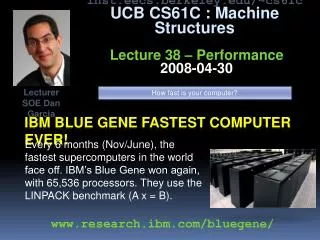
Interconnection and Packaging in IBM Blue Gene/L. Yi Zhu Feb 12, 2007. Outline. Design goals Architecture Design philosophy. Main Design Goals for Blue Gene/L. Improve computing capability, holding total system cost. Reduce cost/FLOP. Reduce complexity and size.

E N D
Interconnection and Packaging in IBM Blue Gene/L Yi Zhu Feb 12, 2007
Outline • Design goals • Architecture • Design philosophy
Main Design Goals for Blue Gene/L • Improve computing capability, holding total system cost. • Reduce cost/FLOP. • Reduce complexity and size. • ~25KW/rack is max for air-cooling in standard room. • 700MHz PowerPC440 for ASIC has excellent FLOP/Watt. • Maximize Integration: • On chip: ASIC with everything except main memory. • Off chip: Maximize number of nodes in a rack..
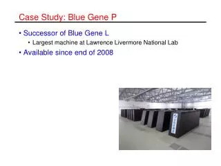
Blue Gene/L Packaging • 2 nodes per compute card. • 16 compute cards per node board. • 16 node boards per 512-node midplane. • Two midplanes in a 1024-node rack. • 64 racks
Dimensions • Compute card: 206 mm x 55 mm • Node card: near to 0.46 m x 0.61 m • Midplane: 0.64m tall x 0.8m x 0.5m • Rack: 2m tall x 0.91 m x 0.91 m
Topology • On one midplane: 16 node cards x 16 computer cards x 2 chips – 8x8x8 torus • Among midplanes: three network switches, one per dimension – 8x4x4 torus
Other Networks • A global combining/broadcast tree for collective operations • A Gigabit Ethernet network for connection to other systems, such as hosts and file systems. • A global barrier and interrupt network • And another Gigabit Ethernet to JTAG network for machine control
Node Architecture • IBM PowerPC embedded CMOS processors, embedded DRAM, and system-on-a-chip technique is used. • 11.1-mm square die size, allowing for a very high density of processing. • The ASIC uses IBM CMOS CU-11 130nm micron technology. • 700 Mhz processor speed close to memory speed. • Two processors per node. • Second processor is intended primarily for handling message passing operations
First Level Packaging • Dimension: 32mm x 25mm • 474 pins • 328 signals for the memory interface • A bit-serial torus bus • A 3-port double-bit-wide bus • 4 global OR signals for fast asynchronous barriers
Computer Cards Bus widths # pins, # ports Design Philosophy • Key: determine the parameters from high-level package to chip pin assignment Interconnection Networks Routing and Pin assignment Card connectors, dimensions
Interconnection Networks • Cables are bigger, costlier and less reliable than traces. • So want to minimize the number of cables. • 3-dimensional torus is chosen as main BG/L network, with each node connected to 6 neighbors. • Maximize number of nodes connected via circuit card(s) only.
Interconnection Networks • BG/L midplane has 8*8*8=512 nodes. • (Number of cable connections) / (all connections) = (6 faces * 8 * 8 nodes) / (6 neighbors * 8 * 8 * 8 nodes) = 1 / 8
Compute Card • Determined by the trade off space, function and cost • Fewest possible computer ASICs per card has lowest cost for test, rework and replacement • Two ASICs per card are more space-efficient due to the share SDRAM
Bus Widths • Bus width of the torus network was decided primarily by # cables that could be physically connected to a midplane • Collective network and interrupt bus widthsand topology were determined by computer card form
# Pins and # Ports • # Pins per ASIC is determined by the choice of collective network and interrupt bus widths + # ports escaping each ASIC • # collective ports per ASIC & between card connectors was a tradeoff between collective network latency and system form factor
Final Choices • 3 collective ports per ASIC • 2 bidirectional bits per collective port • 4 bidirectional global interrupt bit per interrupt bus • 32mmx25mm package • Other factors (computer card form, widths of various buses…) are determined to yield the maximal density of ASICs per rack
Design Philosophy • Next to determine: • Circuit card connectors • Card cross section • Card wiring • Objectives • Compactness • Low cost • Electrical signaling quality
Card-to-Card Connectors • Differential: because all high-speed buses are differential • Two differential signal pairs per column of pins • Signal buses to spread out horizontally across nearly the entire width of each connection • Fewer layers to escape, fewer crosses • Final choice: Metral 4000 connector
Circuit Card Cross Sections • Fundamental requirement: high electrical signaling quality • Alternating signal and ground layers • 14 total layers except the midplane (18 layers) • Node card requires additional power layers to distribute 1.5V core voltage to computer cards
Circuit Card Cross Sections • In some layers with long distance nets, need low resistive loss • Wide (190 um to 215 um) 1.0-ounce copper traces • Other layers, minimize card thickness • Narrow (100 um) 0.5-ounce nets • Card dielectrics: low-cost FR4 • Sufficient for signaling speed 1.4 Gb/s
Card Sizes • Determined by a combination of manufacturability and system form factor consideration • Node cards are near to the maximum card size obtainable from the industry-standard low cost 0.46m x 0.61m • Midplane is confined to the largest panel size that could still be manufactured by multiple card vendors
Card Wiring • Goal: minimize card layers (minimize card cost) • Routing order • 3d torus network (most regular and numerous) on cards • Pin assignment for torus network to minimize net signal crossing
Card Wiring • Routing order (cont’d) • Global collective network & interrupt bus • Exact logical structures determined to minimize # layers • Layout of 16-byte-wide SDRAM • Optimize package escape and # routing layers • ASIC pin assignment • High-speed clocks • Low-speed nets
References • “Overview of the Blue Gene/L system architecture”, IBM J Res. & Dev., Vol. 49, No. 2/3, March/May 2005 • “Packaging the Blue Gene/L supercomputer”, IBM J Res. & Dev., Vol. 49, No. 2/3, March/May 2005 • “Blue Gene/L torus interconnection network”, IBM J Res. & Dev., Vol. 49, No. 2/3, March/May 2005