Download
1 / 26
260 likes | 535 Views
Memory Speculation of the Blue Gene/Q Compute Chip Martin Ohmacht/ IBM BlueGene Team. Acknowledgements. Blue Gene/Q is currently under development by IBM and is not yet generally available. The IBM Blue Gene/Q development teams are located in Yorktown Heights NY, Rochester MN,

E N D
Memory Speculation of the Blue Gene/Q Compute ChipMartin Ohmacht/ IBM BlueGene Team
Acknowledgements • Blue Gene/Q is currently under development by IBM and is not yet generally available. • The IBM Blue Gene/Q development teams are located in • Yorktown Heights NY, • Rochester MN, • Hopewell Jct NY, • Burlington VT, • Austin TX, • San Jose CA, • Bromont QC, • Toronto ON, • Boeblingen (FRG), • Haifa (Israel) • Hursley (UK). • Columbia University • University of Edinburgh • The Blue Gene/Q project has been supported by Argonne National Laboratory and the Lawrence Livermore National Laboratory on behalf of the United States Department of Energy, under Lawrence Livermore National Laboratory Subcontract No. B554331
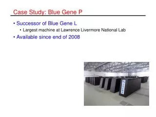
Blue Gene/Q system objectives • Massively parallel supercomputing systems • Focusing on large scale scientific and analytics applications • Broadening to applications with commercial / industrial impact • Laying groundwork for Exascale computing • Reduce total cost of ownership • Power efficient chips power/cooling efficiency dense packaging floor space efficiency • Reliability • Long MTBF for large installations Chip design objectives: • optimize FLOPS/Watt • optimize redundancy / ECC usage / SER sensitivity
BlueGene/Q Compute chip System-on-a-Chip design : integrates processors, memory and networking logic into a single chip • 360 mm² Cu-45 technology (SOI) • ~ 1.47 B transistors • 16 user + 1 service processors • plus 1 redundant processor • all processors are symmetric • each 4-way multi-threaded • 64 bits PowerISA™ • 1.6 GHz • L1 I/D cache = 16kB/16kB • L1 prefetch engines • each processor has Quad FPU (4-wide double precision, SIMD) • peak performance 204.8 GFLOPS@55W • Central shared L2 cache: 32 MB • eDRAM • multiversioned cache will support transactional memory, speculative execution. • supports atomic ops • Dual memory controller • 16 GB external DDR3 memory • 1.33 Gb/s • 2 * 16 byte-wide interface (+ECC) • Chip-to-chip networking • Router logic integrated into BQC chip. • External IO • PCIe Gen2 interface
BG/Q Processor Unit • A2 processor core • Mostly same design as in PowerEN™ chip • Implements 64-bit PowerISA™ • Optimized for aggregate throughput: • 4-way simultaneously multi-threaded (SMT) • 2-way concurrent issue 1 XU (br/int/l/s) + 1 FPU • in-order dispatch, execution, completion • L1 I/D cache = 16kB/16kB • 32x4x64-bit GPR • Dynamic branch prediction • 1.6 GHz @ 0.8V • Quad FPU • 4 double precision pipelines, usable as: • scalar FPU • 4-wide FPU SIMD • 2-wide complex arithmetic SIMD • Instruction extensions to PowerISA • 6 stage pipeline • 2W4R register file (2 * 2W2R) per pipe • 8 concurrent floating point ops (FMA) + load + store • Permute instructions to reorganize vector data • supports a multitude of data alignments QPU: Quad FPU
L1 miss List address address BlueGene/Q PUnit – ct. • L1 prefetcher • Normal mode: Stream Prefetching • in response to observed memory traffic, adaptively balances resources to prefetch L2 cache lines (@ 128 B wide) • from 16 streams x 2 deep through 4 streams x 8 deep • Additional: 4 List-based Prefetching engines: • One per thread • Activated by program directives, e.g. bracketing complex set of loops • Used for repeated memory reference patterns in arbitrarily long code segments • Record pattern on first iteration of loop; playback for subsequent iterations • On subsequent passes, list is adaptively refined for missing or extra cache misses (async events) • Wake-up unit • Will allow SMT threads to be suspended, while waiting for an event • Lighter weight than wake-up-on-interrupt -- no context switching • Improves power efficiency and resource utilization List-based “perfect” prefetching has tolerance for missing or extra cache misses
Crossbar switch • Central connection structure between • PUnits (L1-prefetchers) • L2 cache • Networking logic • Various low-bandwidth units • Half frequency (800 MHz) clock grid • 3 separate switches: • Request traffic -- write bandwidth 12B/PUnit @ 800 MHz (under simultaneous reads) • Response traffic -- read bandwidth 32B/PUnit @ 800 MHz • Invalidate traffic • 22 master ports • PUnits • DevBus master -- PCIe • Network logic ports -- Remote DMA • 18 slave ports • 16 L2 slices • DevBus slave -- PCIe, boot / messaging RAM, performance counters, … • Network logic -- injection, reception • Peak on-chip bisection bandwidth 563 GB/s
L2 structure • 32 MB / 16 way set-associative / 128B line size • Point of coherency • Organization: • 16 slices @ 2MB each • each slice contains 8 * 2.25 Mb eDRAMs (data+ECC)plus directory SRAMs, buffers, control logic. Crossbar switch DEVBUS L2 L2 L2 L2 L2 L2 L2 L2 L2 L2 L2 L2 L2 L2 L2 L2 L2_counter L2_counter L2_counter L2_counter L2_central memorycontroller memorycontroller
Speculation • Code section containing side effects is executed • Side effects are either • made permanent (and visible to other threads), or • side effects are removed and a state restored as if the section was never executed • A successful execution implies atomicity of main memory updates in most proposals event,conflict speculativesection ~ invalidation,revertside effectsof section commit,make side effectspermanent and visible
BG/Q implementation features: • Hardware support for speculative state in memory, not for core registers • Responsibility of software to save and restore state of live registers if necessary • Support for multiple modes: • ordered transactions: • Final value of multiple speculative writes resolved by hardware based on thread order • Forwarding: Younger threads can observe changes caused by older threads while both being speculative • Younger threads need to be invalidated if older thread is invalidated => Speculative Execution • unordered transactions: • Access to state accessed by other transactions considered a conflict if at least one speculative write involved • Threads can commit in any order => Transactional Memory
Rollback / fine grain checkpointing Thread0 Thread1 Thread67 • Snapshot interrupt driven at timer interval or by user call • Live registers or architected core state saved • Changes of previous calculation interval committed • New speculative calculation interval started • Detected error event causes rollback • Changes since last snapshot invalidated • Core restored to last saved state • New speculative calculation interval started • Detection of I/O using speculative data causes commit • No rollback capability until next snapshot • Temporary vulnerability to SER events Calculation … Snapshot SER event SER event ~ ~ Rollback Snapshot
Speculation IDs Avail • Accesses of speculative threads distinguished by short IDs, tagged onto memory access requests by the cores • L2 directory entries marked with IDs to enable multiversioning and conflict detection • IDs are in one of four states:Available, Speculative, Invalid or Committed • State table lookup used when matching tags, allowing instant invalidates/commits by state table change • Directory entries are cleaned up if they contain Ids in committed or invalid state • Removal of lines written using ID in invalid state • Merge of lines written using ID in committed state • clean-up on access and by background scrub • Counter set keeps track of number of references in the directory • When counter reaches zero, ID can be reused for new speculation Allocation Spec Commit Abort Invalid Committed Reclaim
Ordering • BG/Q provides 128 IDs, numbered 0 to 127 • Numeric value of ID determines order • Generally, larger values indicate younger threads • ID value space wraps • Allocation pointer used in comparisons • ID space can be divided into up to 16 groups (domains): • Each domain provides independent allocation pointer, allowing independent ordering • Each domain can be assigned a different mode, allowing concurrent ordered and unordered transactions • IDs can be assigned to any hardware thread
Implementation • Up to 15 ways of each directory set can be used for speculative data • Up to 30MB speculative space • Number of speculative ways protected from eviction configurable • Write accesses recorded down to 8B granularity, reusing coherence directory space • Read accesses recorded with dynamically determined granularity, 8B best case
L2 cache -- continued • Atomic operations • Can be invoked on any 64-bit word in memory • Atomic operation type is selected by unused physical address bits • Set of 16 operations, including fetch-and-increment, store-add, store-XOR, etc. • Some operations access multiple adjacent locations, e.g., fetch-and-increment-bounded • Low latency even under high contention • avoids L2-to-PU roundtrip cycles of lwarx/stwcx -- “queue locking” s/w operations: locking, barriers • efficient work queue management, with multiple producers and consumers • efficient inter-core messaging
DDR3 memory interface • L2 cache misses are handled by dual on-chip DDR3 memory controllers • each memory controller interfaces with 8 L2 slices • Interface width to external DDR3 is 2 * (16B + ECC) • aggregate peak bandwidth is 42.7 GB/s for DDR3-1333. • Designed to support multiple density/rank/speed configurations • currently configured with 16GB DDR3-1333 • DRAM chips and BQC chip soldered onto same card • eliminates connector reliability issues • reduces driver and termination power • Extensive ECC capability on 64B basis: • Double symbol error correct / triple detect -- symbol = 2bits * 4 beats. • Retry • Partial or full chip kill • DDR3 PHY • integrated IO blocks: 8bit data + strobe; 12 /16 bit address/command • integrates IOs with delay lines (deskew), calibration, impedance tuning, …
Networking logic • Communication ports: • 11 bidirectional chip-to-chip links @ 2GB/s • Implemented with High Speed Serial (HSS) cores • 2 links can be used for PCIe Gen2 x8 • On-chip networking logic • Implements 14-port router • Designed to support point-to-point, collective and barrier messages • Integrated floating point and fixed point arithmetic, bit-wise operations • Integrated DMA: connects network to on-chip memory system • With these hardware assists, most aspects of messaging will be handled autonomously • Minimal disturbance of PUnits
The 17th Core • Assistant to the 16 user cores • Designed to handle Operating System services • Planned usage: • Offload interrupt handling • Asynchronous I/O completion • Messaging assist, e.g. MPI pacing • Offload RAS Event handling • Reduces O/S noise and jitter on the user cores • Will help user applications to run predictably / reproducibly
Redundancy – the 18th core Scan chain arrangement designed for simple determination of PUnit logic fails at manufacturing test
Physical-to-Logical mapping of PUnits in presence of a fail used shut down • Inspired by array redundancy • PUnit N+1 redundancy scheme designed to increase yield of large chip • Redundancy can be invoked at any manufacturing test stage • wafer, module, card, system • Redundancy info will travel with physical part -- stored on chip (eFuse) / on card (EEPROM) • at power-on, info transmitted to PUnits, memory system, etc. • Single part number flow • Will be transparent to user software: user will see N consecutive good processor cores.
4. Node Card 32 Compute Cards, Optical Modules, Link Chips, Torus Blue Gene/Q packaging hierarchy 3. Compute Card One single chip module, 16 GB DDR3 Memory 2. Module Single Chip 1. Chip 16 cores 5b. I/O Drawer 8 I/O Cards 8 PCIe Gen2 slots 7. System 20PF/s 6. Rack 2 Midplanes 1, 2 or 4 I/O Drawers 5a. Midplane 16 Node Cards Ref: SC2010
Design Challenges • Area is the enemy • 16 processor cores (A2 + QPU + L1P) + 1 helper core + 1 redundant spare • enough cache per core / per thread • high bandwidth to/from cache and to external memory • high speed communication • leads to LARGE chip: 18.96x18.96 mm redundant processor core will significantly help yield • Power is the enemy • SOC design (processors, memory, network logic) reduces chip-to-chip crossings • 2.4 GHz PowerEN™ core design is run at reduced speed (1.6 GHz), reduced voltage (~0.8V) • reduced voltage will reduce both active power and leakage power • speed binning all chips run @ 1.6 GHz, with voltage adjusted to match speed sort. • Deployed methodologies/tools to keep power down • Architecture/logic level: clock gating • Processor cores: re-tuned for low power • Power-aware synthesis; power-recovery steps • Physical design: power-efficient clock networks • Soft Errors are the enemy • Sensitivity to SER events will affect reliability for large installations – such as BlueGene/Q • Design provides redundancy for data protection: • DDR3, L2 cache, network, all major arrays and buses ECC protected • Minor buses, GPRs, FPRs: parity protected, with recovery • Stacked / DICE latches
Design Challenges -- continued And the enemy is us… • Methodology Complexity • Processor cores originated in a high-speed custom design methodology • Rest of the chip implemented as ASIC Required merging of different clocking/latching, timing and test methodologies • Logic verification • On-chip memory sub-system (transactional memory, speculative execution) • Full-chip POR sequence, X-state (… inherited “proven” logic) Extensive use of cycle simulation / hardware accelerators / FPGA emulator • Test pattern generation • Again, mixed chip / mixed methodologies • Full chip models • turn-around time is becoming a bottleneck
Conclusions • The Blue Gene/Q Compute chip will be the building block for a power-efficient supercomputing system that will be able to scale to tens of PetaFLOPS. • Hardware • BQC will introduce architectural innovations to enable multithreaded / multicore computing • Cache structure designed to support Speculative Execution and Transactional Memory • On-chip networking logic will allow dense, high-bandwidth chip-to-chip interconnect, with hardware assist for collective functions and RDMA • Designed to achieve over 200 GFLOPS peak in a power-efficient fashion 2.1 GFLOPS/W Linpack performance -- #1 in Green500 June 2011 • Software • Processors are homogeneous, implement standard PowerISA (plus SIMD extensions) • Compilers will be available that leverage the on-chip hardware assists for multithreading • Plan to support open standards: • Parallel processing: MPI • Multi-threading: OpenMP … and will allow for many other programming models • Applications: • are in bring-up / scale-up
Disclaimer IBM Corporation Integrated Marketing Communications, Systems & Technology Group Route 100 Somers, NY 10589 Produced in the United States of America 07/15/2011 All Rights Reserved IBM’s statements regarding its plans, directions, and intent are subject to change or withdrawal without notice at IBM’s sole discretion. Information regarding potential future products is intended to outline our general product direction and it should not be relied on in making a purchasing decision. The information mentioned regarding potential future products is not a commitment, promise, or legal obligation to deliver any material, code or functionality. Information about potential future products may not be incorporated into any contract. The development, release, and timing of any future features or functionality described for our products remains at our sole discretion. Some information in this document addresses anticipated future capabilities. Such information is not intended as a definitive statement of a commitment to specific levels of performance, function or delivery schedules with respect to any future products. Such commitments are only made in IBM product announcements. The information is presented here to communicate IBM’s current investment and development activities as a good faith effort to help with our customers’ future planning. All performance information was determined in a controlled environment. Actual results may vary. Performance information is provided “AS IS” and no warranties or guarantees are expressed or implied by IBM. IBM does not warrant that the information offered herein will meet your requirements or those of your distributors or customers. IBM provides this information “AS IS” without warranty. IBM disclaim all warranties, express or implied, including the implied warranties of noninfringement, merchantability and fitness for a particular purpose or noninfringement.
Disclaimer References in this publication to IBM products or services do not imply that IBM intends to make them available in every country in which IBM operates. Consult your local IBM business contact for information on the products, features, and services available in your area. Blue Gene, Blue Gene/Q and PowerEN are trademarks or registered trademarks of IBM Corporation in the United States, other countries or both. PowerISA and Power Architecture are trademarks or registered trademarks in the United States, other countries, or both, licensed through Power.org Linux is a registered trademark of Linus Torvalds. Tivoli is a registered trademark of Tivoli Systems Inc.in the United States, other countries or both. UNIX is a registered trademark in the United States and other countries, licensed exclusively through The Open Group. Other trademarks and registered trademarks are the properties of their respective companies. Photographs shown are of engineering prototypes. Changes may be incorporated in production models. This equipment is subject to all applicable FCC rules and will comply with them upon delivery. IBM makes no representations or warranties, expressed or implied, regarding non-IBM products and services.