Download
1 / 20
360 likes | 842 Views
MATERIAL SCIENCE ASSIGNMENT. SCANNING ELECTRON MICROSCOPE. BY SANTANU PRAMANIK(09369) HITESH KUMAR GUPTA(09320) CHANDAN SINGH(09260). History. TEM constructed in 1931 Von Ardenne first STEM in 1938 by rastering the electron beam in a TEM Zworykin et al. 1942, first SEM for bulk samples

E N D
MATERIAL SCIENCE ASSIGNMENT SCANNING ELECTRON MICROSCOPE BY SANTANU PRAMANIK(09369) HITESH KUMAR GUPTA(09320) CHANDAN SINGH(09260)
History • TEM constructed in 1931 • Von Ardenne first STEM in 1938 by rastering the electron beam in a TEM • Zworykin et al. 1942, first SEM for bulk samples • 1965 first commercial SEM by Cambridge Scientific Instruments Resolution at that time ~ 50 nm : Today < 1 nm Morphology only at that time : Today analytical instrument
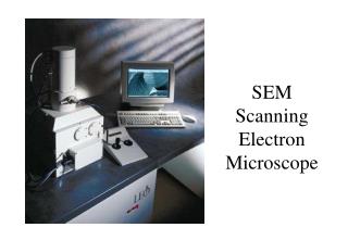
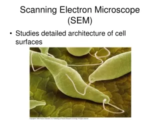
What is SEM? • It is a microscope that produces an image by using an electron beam that scans the surface of a specimen inside a vacuum chamber. What can we study in a SEM? • Topography and morphology • Chemistry • Crystallography • Orientation of grains • In-situ experiments: • Reactions with atmosphere • Effects of temperature “Easy” sample preparation!! “Big” samples!
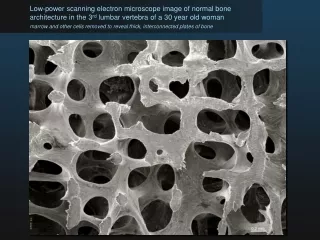
What does it looks like…. AFM Cantilever Tip Ant Head Blood Cells Diamond Thin Film (Numerous Multifaceted Micro-crystals) Microstructure of a plain carbon steel that contains 0.44 wt% of carbon Calcium Phosphate Crystal
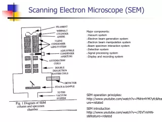
Components of the instrument • electron gun (filament) • electromagnetic optics • scan coils • sample stage • detectors • vacuum system • computer hardware and software (not trivial!!)
Electron guns • We want many electrons per time unit per area (high current density) and as small electron spot as possible • Traditional guns: thermionic electron gun (electrons are emitted when a solid is heated) • W-wire, LaB6-crystal • Modern: field emission guns (FEG) (cold guns, a strong electric field is used to extract electrons) • Single crystal of W, etched to a thin tip
Our traditional detectors Detectors Backscattered electron detector: (Solid-State Detector) Secondary electron detector: (Everhart-Thornley) • Secondary electrons: Everhart-Thornley Detector • Backscattered electrons: Solid State Detector • X-rays: Energy dispersive spectrometer (EDS)
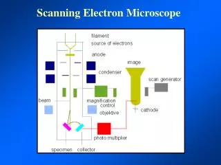
HOW THE SEM WORKS? • The SEM uses electrons instead of light to form an image. • A beam of electrons is produced at the top of the microscope by heating of a metallic filament. • The electron beam follows a vertical path through the column of the microscope. It makes its way through electromagnetic lenses which focus and direct the beam down towards the sample. • Once it hits the sample, other electrons • ( backscattered or secondary ) are ejected from the sample. Detectors collect the secondary or backscattered electrons, and convert them to a signal that is sent to a viewing screen similar to the one in an ordinary television, producing an image.
How do we get an image? Electron gun 156 electrons! 288 electrons! Detector Image
Electron beam-sample interactions • The incident electron beam is scattered in the sample, both elastically and inelastically • This gives rise to various signals that we can detect (more on that on next slide) • Interaction volume increases with increasing acceleration voltage and decreases with increasing atomic number
Signals from the sample Incoming electrons Secondary electrons Auger electrons Backscattered electrons Cathodo- luminescence (light) X-rays Sample
Where does the signals come from? • Diameter of the interaction volume is larger than the electron spot • resolution is poorer than the size of the electron spot
Secondary electrons (SE) • Generated from the collision between the incoming electrons and the loosely bonded outer electrons • Low energy electrons (~10-50 eV) • Only SE generated close to surface escape (topographic information is obtained) • Number of SE is greater than the number of incoming electrons • We differentiate between SE1 and SE2
SE1 • The secondary electrons that are generated by the incoming electron beam as they enter the surface • High resolution signal with a resolution which is only limited by the electron beam diameter SE2 • The secondary electrons that are generated by the backscattered electrons that have returned to the surface after several inelastic scattering events • SE2 come from a surface area that is bigger than the spot from the incoming electrons resolution is poorer than for SE1 exclusively SE2 Incoming electrons Sample surface
Backscattered electrons (BSE) • A fraction of the incident electrons is retarded by the electro-magnetic field of the nucleus and if the scattering angle is greater than 180° the electron can escape from the surface • High energy electrons (elastic scattering) • Fewer BSE than SE • We differentiate between BSE1 and BSE2
BSE vs SE • SE produces higher resolution images than BSE • By placing the secondary electron detector inside the lens, mainly SE1 are detected • Resolution of 1 – 2 nm is possible
X-rays • Photons not electrons • Each element has a fingerprint X-ray signal • Poorer spatial resolution than BSE and SE • Relatively few X-ray signals are emitted and the detector is inefficient • relatively long signal collecting times are needed
Some comments on resolution • Best resolution that can be obtained: size of the electron spot on the sample surface • The introduction of FEG has dramatically improved the resolution of SEM’s • The volume from which the signal electrons are formed defines the resolution • SE image has higher resolution than a BSE image • Scanning speed: • a weak signal requires slow speed to improve signal-to-noise ratio • when doing a slow scan drift in the electron beam can affect the accuracy of the analysis
References • Fundamentals of materials Science and Engineering – William D. Callister • Physical Metallurgy – Robert W. Cahn • Physical Metallurgy and Advanced Materials – R. E. Smallman • Physical Metallurgy Principles – Robert E. Reedhill • http://en.wikipedia.org/scanning_electron_microscope Thank You