Download
1 / 30
320 likes | 551 Views
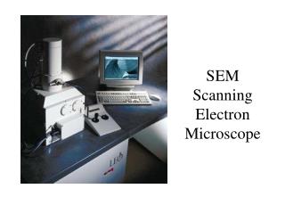
Studying micro-objects with SEM (Scanning electron microscope). Student: Michał Łępicki (Warsaw University of Technology ) Supervisor : Oleg Leonidovich Orelovich Center of Applied Physics of Flerov Laboratory of Nuclear Reactions JINR. Introduction. Introduction. Introduction.

E N D
Studying micro-objects with SEM (Scanning electron microscope) Student: Michał Łępicki (Warsaw University of Technology) Supervisor: Oleg Leonidovich Orelovich Center of Applied Physics of Flerov Laboratory of Nuclear Reactions JINR
Program of practices • Layout and performance of SEM • Preparing and coating samples • Operating SEM • Electron data processing
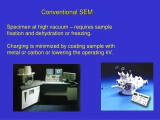
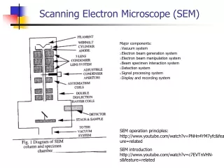
Layout and performance of SEM 1-3 Electron gun 4, 10 Aperture 5-6 Condenser lenses 7 Scanning coils 8 Stigmator 9 Objective lens 11 X-ray detector 12 Pre-amplifier 13 Scanning circuits 14 Specimen 15 Secondary electron detector 16-18 Display/Control circuits
Preparing and coating samples General view of ion sputter
Reasons of coating specimens • The surface of sample must be electro conductive to minimalize charging from beam • The surface must be thermo conductive to minimalize local heating • The material of sample must have a high atomic number to increase secondary electron emission
Preparing and coating samples Gold coated sample Sample without coating
Preparing and coating samples Tilt 0 deg – shadowless illumination Tilt 30 deg
TILT Operating SEM Tilt 30 deg Tilt 0 deg
A/D Electron data processing
Electron data processing N=1,75*10^7 [channels/cm^2] R=0,5μm average channel radius 13,8% surface cross section (SCS) SCS= Pi*R^2*N*100%