Download
1 / 67
680 likes | 689 Views
BMFB 3263Material Characterisation Scanning Electron Microscope (SEM). Light microscope – limited by wavelength of light. Electron microscope – much lower wavelength allows resolution a thousand times better. SEM. TEM. Topic outcomes. By the end of this topic, students should be able to

E N D
BMFB 3263Material CharacterisationScanning Electron Microscope (SEM)
Light microscope – limited by wavelength of light. • Electron microscope – much lower wavelength allows resolution a thousand times better. SEM TEM
Topic outcomes By the end of this topic, students should be able to • List down the differences between optical microscope and electron microscope • Acknowledge the importance of electron microscope for materials engineers and scientists • Describe most important parts of SEM, and their roles in obtaining high quality image • Explain typical sample preparation for metals, ceramic, polymers and films
250x, Al alloy 356 casting showing primary α and eutectic phase. SEM micrograph of same alloy, shows shrinkage cavity (other microstructure features like grain boundaries is not shown).
Al alloy reinforced with SiC particles imaged with OM and SEM .
ZnO Nanowires by Anodisation at Our Lab Anodisation of Zn Nanoflowers ZnO Anodisation of Zn Nanoneedles ZnO NanoPorous ZnO
Optical microscope vs SEM Magnification limit is a function of wavelength of visible light, 2000 Å. Wavelength of electrons < 0.5 Å gives theoretical max magnification of 800,000x. Resolving power OM is limited by wavelength of light. In light microscope, quality of objective lens also plays major role in determining resolving power. Resolving power – ability to optically separate 2 objects. Limiting conditions for transmitting info using electromagnetic radiation – key parameter is ratio /d.
Electron Microscope EM is developed because wavelength has an effective role on theoretical resolution. Green light used for light microscope has wavelength of 0.5 µm, & thus theoretical resolution of 0.2 µm. Followed by blue, violet & ultraviolet. But ultraviolet is absorbed by glass. X-ray ? Cannot be easily refracted to form image. Inability to focus the rays. Electron – could easily be focused by magnetic field. De Broglie postulate ‘dual nature of electrons – particle & wave’. Also can be accelerated by electrical potential.
Factors influence key parameters of performance for SEM • Depth of field • Imaging noise • Resolution
2 general types of SEM • Typical SEM • Samples must be dried before hand • Must be coated with conductive coating e.g. gold, Pt • Environmental SEM • For biological samples • Do not have to dry the samples
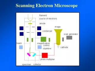
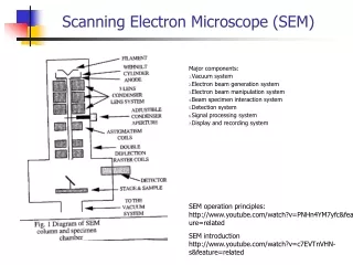
(a) Schematic diagram of SEM, (b) Ray paths in SEM-standard arrangement for image formation
Electron Microscope Another limit of light m/scope is depth of field – distance from nearest to farthest part of subject that is in focus when picture is taken. Depth of field – ability to maintain focus across a field of view regardless of surface roughness. SEM can maintain 3D appearance of textured surface. Advantage of electron m/scope – increase in depth of field and depth of focus. SEM also usually equipped with EDX or X – ray mapping to determine chemical composition at a particular spot.
Electron Microscope – basic principle Focusing is possible because of dual-nature of electrons. De-Broglie relationship : = h/mv where m – mass, v is velocity & h is Planck constant. Electrons are deflected by both electrostatic & magnetic fields and can be brought to a focus by engineering the field geometry. EM – virtual source of electrostatic field by anode & subsequent focus by electromagnetic lenses. Cathode filament generates electrons and accelerated by potential difference between anode & filament. Shield serves to collimate electrons & direct them.
Scanning Electron Microscope (SEM) Study topography of solid samples, resolution around 0.3 µm to 0.15 nm. A source of high energy electrons, condenser system and probe lens to focus the electron beam into fine probe that impinges on specimen. Image is obtained by scanning the electron probe over surface and collect image signal – display after suitable amplification and processing. Sample : electrically conductive, nonconductive materials require thin conductive coating to prevent electrical charging of the specimen.
Scanning Electron Microscope (SEM) An energetic electron penetrating solid sample undergoes both elastic & inelastic scattering. Inelastic predominates, reducing energy in beam to kinetic energy kT. Release of secondary electron emission from surface generate electron current in sample due to impact of high energy incident beam. Si-dioxide nanoparticle
Scanning Electron Microscope (SEM) In SEM, a fine beam of electrons is scanned across surface of sample, a detector counts the number of low energy secondary electrons, or other radiation, emitted from each point of the surface. The brightness of each image pixel is modulated according to the output current of the detector for each point of surface and an image is build up in this way as the beam scans. Because secondary electrons come from near surface region, the brightness of signal depends on surface area that is exposed to the primary beam.
1. Depth of field e- beam converging to the image plane with semi-angular aperture , where d is the resolution required and D is the depth of field for SEM
Depth of field • DoF- represent the distance along microscope axis over which the specimen can be displayed within the blurring image • For a beam of a fixed divergence angle , blurring is measured by the diameter of the ‘disc of confusion’, d, which is related to to the axial shift, D, where (D/2) tan =d/2
Depth of field and resolution of the SEM (final aperture 5 x 10⁻³ rad) compared with that achieved by the optical light microscope
Noise • Noise within image present in all forms • Related to collecting efficiency of the imaging system • Noise influences the resolution • In SEM, resolution is improved if • the signal is collected for longer periods of time • Increase the contrast
Electron sources • In SEM, incident e- is focused on the specimen, • but sometimes it is also scanned over the specimen • Resolution is set by the diameter of incident beam and mode of operation • Important thing: minimise energy spread within the electron beam, to minimise chromatic aberration • Electron sources influence: • Brightness • Quality of image being obtained
Scanning Electron Microscope (SEM) Electron beam source – tungsten or lanthanum hexaboride LaB6 cathode filament. Alternative – via field emission (FE). Beam is focused by two successive condenser lenses into beam with very fine spot size (~ 5nm). Condenser aperture – eliminate high angle electrons. Objective aperture – further eliminate high-angle electrons. Beam then passes thru objective lens where pairs of coils scan the beam in grid or raster fashion over rectangular area of surface.
Scanning Electron Microscope (SEM) Beam diameter / spot size – one of the most important parameters, and it is controlled directly by operator electromagnetic probe lens or objective lens. Focus achieved by varying current passing thru objective lens. Charging - manifested as bright streaks or flashes across width of photograph, observed when spot size is excessively large. Results when specimen accumulates a net negative charge. Non-conductive samples examined at excessive accelerating voltage, contaminants particles or films.
Scanning Electron Microscope (SEM) Reduce charging – coat with gold or carbon, connect to ground with conductive adhesive, clean properly. Inelastic collision (electron – electron) secondary electrons, X-ray, phonon (heat). Elastic collision (electron – nucleus) produce backscattered electrons (BSE). If mean atomic wt (Z) of specimen is low, e.g plastic, probability of backscattering event is lower than if Z is higher. So high-Z metal release greater number of BSE than low Z specimens. BSE imaging distinguish zones of different Z material.
Comparison of the performance for different electron sources
Filament SEM Filament is much smaller than this
Resolution • Resolution- critical parameters which governs the performance of a SEM • Resolution is a balance between the effects of aberration of the final lenses and diffraction effects • Most SEM has at least 5nm resolution • Ultra high resolution SEM: provide smallest diameter and brightest electron source combine with ability to the detect secondary the emitted secondary electrons with the highest efficiency
Imaging modes 3 main methods to collect emitted electron signals • Secondary electron • Backscattered electrons • Absorbed specimen current
Photomultiplier system to detect the secondary electrons Methods of detecting e- in SEM; (a) Secondary electron, (b) Backscattered electron, scintillation counter
Absorbed electron current Backscattered electrons scintillation counter
3 most commonly used SEM imaging modes together with resolution attainable
Secondary electron emission at surface irregularities: contributions from specimen collection are indicated • Specimen with pronounced surface roughness, contrast is modified by surface collection contributions • Any improved contrast is usually accompanied by degradation of image details
Secondary electrons images, (a) fracture of steel, (b) low alloy ferritic steel steam pipe after operation, (c) rapidly cooled polyethelene where morphology in the centre is revealed as a consequence of damage by incident beam
Scanning Electron Microscope (SEM) Back-scattered electron detection gives rise to images presenting a compositional contrast (BSE yield being a function of atomic number). Different atomic number gives different contrast. As primary electron strike the surface they are inelastically scattered by atoms in sample. Interactions lead to emission electrons – detected to produce image. X-rays, which also produced by this interaction may also be detected in SEM equipped for Energy Dispersive X-ray Spectroscopy (EDX).
Scanning Electron Microscope (SEM) Factors directly affect SE emission from surface : Work function of surface (energy supplied for electron to escape), depends on both composition & atomic packing. Beam energy & intensity. Density of sample (limited influence). Surface topography (most pronounced effect) or local curvature of surface. FE SEM – capable of nm resolutions at beam energies as low as 200 V, and give excellent contrast based on either atomic number or work function. Alternative imaging – cathodoluminescence & electron beam image current.
Scanning Electron Microscope (SEM) Working distance (WD) – distance separating surface from final pole piece. Short WD – decreases depth of field, raises lower limit of magnification, may reduce image clarity by interfering with SE collection, & may limit sample movement. Long WD – enhances DoF, permits low mag, but also reduces image clarity coz electron signals have to travel farther for detection. Energy dispersive Spectroscopy (EDS) – detect X-rays emitted by specimen.
Scanning Electron Microscope (SEM) Every elements has their own characteristic energy and wavelength pattern. Limitation not able to detect - light elements (C, N, O), specifically identify compounds or ionic state of detected element. But new tech able to detect light elements down to boron (Z = 5) for quantitative. X-ray signal mode of display : spectrum, line scan & X-ray dot image or elemental map. X-ray dot – characteristic photon recorded as white dot.
EDS X-ray spectrum from small Ti carbonitride particle in Al. (a) Al metal, (b) TiCN particle
Wavelength-dispersive spectrometry : The line profiles for nickel, chromium, silicon, and manganese in a specimen of cast iron. One can see that the silicon and nickel are associated, as are the chromium and manganese. Line analyses can then be calibrated with quantitative analyses.
Sample preparation • Surfaces of the bulks of metals, polymers, ceramics • Cutting, etching or fracturing- depends on what kind of information we want to observe. • Examples: • If we want to observe grains, grains boundaries, open pores structure: • Similar with sample preparation for optical microscope
Scanning Electron Microscope (SEM) Sample preparation – electrostatic charging should be avoided. Coating – sputtering of heavy metal such as gold-palladium or carbon. Carbon is usually more desirable when EDS is used so as not to interfere with chemical analysis. Fractography and failure analysis – surface should NOT be damaged or altered in any way by any prior specimen preparation procedure. Spatial & orientational relationship to component must be known, images recorded over full range.