Download
1 / 43
430 likes | 444 Views
CBM MVD Detector and 3D Integration Processes. Review of the 15th CBM Collaboration Meeting and the VIPS2010 Workshop. Shiming Yang 06.05.2010. Outline. MVD Detector of CBM experiment Brief introduction, specifications Request for the 3D integrated CMOS pixel sensor Nowaday status of MVD

E N D
CBM MVD Detector and 3D Integration Processes Review of the 15th CBM Collaboration Meeting and the VIPS2010 Workshop ShimingYang 06.05.2010
Outline • MVD Detector of CBM experiment • Brief introduction, specifications • Request for the 3D integrated CMOS pixel sensor • Nowaday status of MVD • 3D Integration technology • Introduction • Development of 3D Integrated pixel sensors • Industry Activities • Designs for high energy physics • Conclusion
CBM Experiment CBM experiment at FAIR Staszel, Pawel,Jagiellonian University, Krakow Text.Article,Published: 2010-01-01
MVD Detector Two configurations of the CBM detector are being evaluated for electron-hadron and muon hadron measurements. Both may be realized at different stages. They have in common a lowmass silicon tracking system (STS), the central detector to perform charged-particle tracking and high-resolution momentum measurement with radiation tolerant silicon microstrip and pixel detectors. Combined with an ultra-thin micro-vertex detector (MVD) based on monolithic active pixel sensors, it will be installed in the gap of a dipole magnet in short distance downstream of the target. The Compressed Baryonic Matter Experiment at FAIR: Progress with feasibility studies and detector developments Heuser, Johann;GSI, Darmstadt Text.Article, Published: 2009-11-10
MVD Detector Development of fast and radiation hard Monolithic Active Pixel Sensors (MAPS) optimized for open charm meson detection with the CBM - vertex detector Michael Deveaux, PhD Thesis.
δ- electrons produced in the target z Target (Gold) Detector2 Detector 1 BEAM Primary Beam: 25 AGeV Au Ions (up to 109/s) Dose [neq / cm2 / coll.] Primary vertex Secondary vertex Short lived particle D0 (ct = ~ 120 µm) Reconstruction concept for open charm mm mm The challenge of open charm detection 1013 -1015 neq/cm²/year • Reconstructing open charm requires: • Excellent secondary vertex • resolution (~ 50 µm) • => Excellent spatial resolution (~5 µm) • => Very low material budget (few 0.1 % X0) • => Detectors in vacuum • A good time resolution to distinguish • the individual collisions • Very good radiation tolerance against • >> 1013 neq / cm² / year
Specifications • The vertex detector has to provide a secondary vertex resolution of 50 um. • The granularity and readout speed of the detector have to be sufficient to sense a particle flux of up to 3*109 charged particles per cm2 and second. • To avoid event pile-up, the detector has to have a sucient time resolution to separate the individual nuclear collisions, which appear after a mean time of 100 ns at the nominal luminosity of FAIR. • The detector has to resist to the radiation caused by a particle ux above 1015 articles per cm2 and year at its most irradiated points. • Preliminary! Development of fast and radiation hard Monolithic Active Pixel Sensors (MAPS) optimized for open charm meson detection with the CBM - vertex detector Michael Deveaux, PhD Thesis.
Requirements on radiation hardness Non-ionizing: At the border of the beam hole of the detector stations at 5 cm distance from the target, there will be up to 2 · 10^15 neq /cm^2 per year. Ionizing: In the hottest regions of the MVD, the total ionizing dose may reach 340 MRad. Conceptual design of a 3D integrated pixel detector for the CBM MVD Torheim, Olav, Bergen University Text.Presentation,Published: 2010-04-13
3D Integration Needed Conclusion on requirements Recently new technology like 3D integration and sensors with fully depleted epi opens the perspective of running the CBM at a collision rate of 10^6 collisions per second. A conceptual design for a detector based on this technology, and targeted for CBM at 10^6 collisions per second, is therefore to be presented: Detector tier: XFAB 0.6, bonded to amplifier tier with iptronix DBI Analog amplifier tier: Tezzaron/Chartered Digital tiers: Tezzaron/Chartered Conceptual design of a 3D integrated pixel detector for the CBM MVD Torheim, Olav, Bergen University Text.Presentation,Published: 2010-04-13
Lessons learned TPG= Thermal Pyrolytic Graphite RVC=Reticulated Vitreous Carbon • First implementation with TPG and RVC. • Lessons learned: The sandwich is light, heat conductive, stable but: • TPG is soft, difficult to thin below 150 µm • RVC tends to emit carbon grains • Gluing with very thin films is difficult • Heat management was limited by copper heat sink (weak interface towards TPG and cooling liquid. • Total material budget ~ 2% X0, (1% X0 with thin sensors) M. Deveaux, VIPS 2010 , 22-24th April 2010, Pavia, Italy
~ 60(1) -150(2) µm Si Diamond 200-300 µm < 200 µm Si ~ 60(1) -150(2) µm Si ~ 320(1)-500(2) µm Si Towards the MVD: EU FP7 HadronPhysics2 “ULISI” Build an ultra thin ladder. Partners: IPHC, IKF, IMEC Polyamide Metal lines Sensor (1) first MVD station (2) last MVD station M. Deveaux, VIPS 2010 , 22-24th April 2010, Pavia, Italy
MVD Status-Our Contribution • A concept for a detector used to equip the first station of the MVD is proposed, utilizing and synthesizing the following techniques and technologies: • Fully depleted epi layer, now commercially available, to improve radiation hardness and signal to noise ratio, based on concepts already validated with MIMOSA25. • Zero suppression techniques, based on concepts already validated with MIMOSA26, to reduce data stream. • Rolling shutter operation to limit power consumption, based on concepts to be validated with a design submitted in the first 3D MPW By Torheim, Olav
Closeout - Outlook Senger, Peter GSI, Darmstadt
What’s 3D? Design and implementation of fast and sparsified readout for Monolithic Active Pixel Sensors Olav Torheim,PHD Thesis
Why 3D? Continuing Moore Law
Who wants 3D? • Applications of particular interest to industry includes small form factor and high capacity memories for portable devices like mobile phones. Memories with low activity - and hence, low power dissipation - are ideal 3D integrated applications, Another example is stacking of memory and processor on top of each other in order to bridge the processor-memory performance gap. • For high energy physics, 3D integration provides opportunities of designing detectors where the pixel cell is composed as a 3D stack with separate detector tier1, analog signal conditioning and processing tier, and one or more digital tiers for storage and readout. Each function can be manufactured in the most optimal process, and with the increasing amount of logic per pixel, fast readout architectures with data sparsication can be developed. • Physicist’s Dream.
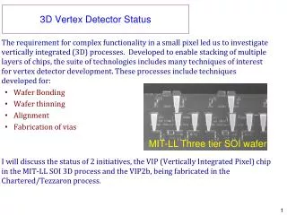
How to 3D?_key factors • Wafers from different processes • TSV fabrication • Alignment • Interconnect, Binding • Thinning
Who offers 3D? • At the present time there are three known vendors that can provide all of the steps needed for fabrication of 3D integrated circuits. More information on these organizations can be found on the following pages. Other vendors such as RTI and IZM can provide a few of the steps and might be considered for some applications. • MIT Lincoln Labs • Tezzaron • Ziptronix T-Micro (SOI)
VIPS2010 Vertical integration (3D for short) processes and vertical interconnect techniques are being explored by industry for several applications, such as memories, pixel sensor arrays, microprocessors and FPGAs. They are deemed capable to make up for some important performance limitation facing CMOS feature size scaling. Digital circuits, in particular, may greatly benefit from interconnect length reduction both in terms of power dissipation and logical span of control. In the case of a heterogeneous integration approach, separate parts of the design can be manufactured using the process that best suits its specific needs, then assembled in a vertical stack. In general, the 3D approach enables the design of low mass, high density circuits with the possibility of isolating the various building blocks, for instance analog from digital parts. The workshop aims to bring together physicists and engineers working on the development of vertically integrated pixel sensors. Particular attention is paid to detector design for high energy physics (HEP) experiments at the future high luminosity colliders and for photon science applications. The main purpose of the workshop is to provide a place for the people working in the field to exchange ideas and share knowledge, and to make the community aware of the different options available to access vertical integration technologies.
VIPS2010-talks • 3D activities in the microelectronic industry and application perspectives • R&D activities in Europe • Activities in the 3DIC Consortium • 3D activity in SOI technology • Latest developments involving vertical integration processes, 3D electronics, mechanics, optics, interposers
SOI Technology http://3dic.fnal.gov/DetectorSOI.pdf
Can’t fully Cover • For details, please refer to the original documents……
Documents and References • Can’t fully Cover all • For details, please refer to the original document. • 15th CBM Collaboration Meeting • http://www-aix.gsi.de/conferences/CBM2010_Apr/ • https://www.gsi.de/gds/?sessionid=1272976685&folder=9871269661485&mod=adminbrowse • VIPS 2010 - Workshop on Vertically Integrated Pixel Sensors • http://eil.unipv.it/MaKaC/conferenceDisplay.py?confId=0 • 3DIC at Fermilab • http://3dic.fnal.gov/
Conclusion • 3D is a fairly new technologies, we are not familiar, interest from HEP. • Many processes, need to be investigated further more by industry and scientific groups. • A new design for high speed readout MAPS for CBM, which we will contribute the digital part.
Attributions belong to the original contributors. All mistakes are mine! • Thanks for your attention! • If questions, I will try to answer ^^.