Download
1 / 41
420 likes | 442 Views
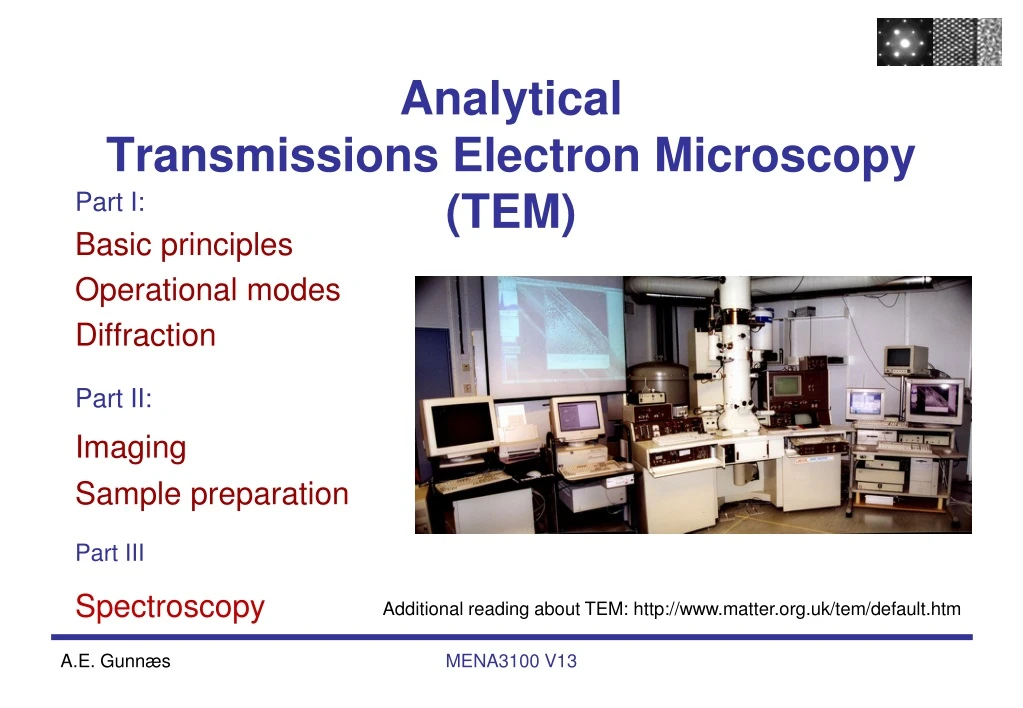
Analytical Transmissions Electron Microscopy (TEM). Part I: Basic principles Operational modes Diffraction Part II: Imaging Sample preparation Part III Spectroscopy. Additional reading about TEM: http://www.matter.org.uk/tem/default.htm. 200 nm.

E N D
Analytical Transmissions Electron Microscopy (TEM) Part I: Basic principles Operational modes Diffraction Part II: Imaging Sample preparation Part III Spectroscopy Additional reading about TEM: http://www.matter.org.uk/tem/default.htm MENA3100 V13
200 nm TEM is based on three possible set of techniqes Spectroscopy Imaging Diffraction Chemistry and elecronic states (EDS and EELS). Spatial and energy resolution down to the atomic level and ~0.1 eV. With spatial resolution down to the atomic level (HREM and STEM) From regions down to a few nm (CBED).
Introduction EM and materials The interesting objects for TEM is not the average structure or homogenous materials but local structure and inhomogeneities Defects Interfaces Precipitates
The first electron microscope • Knoll and Ruska, first TEM in 1931 • Idea and first images published in 1932 • By 1933 they had produced a TEM with two magnetic lenses which gave 12 000 times magnification. Ernst Ruska: Nobel Prize in physics 1986 Electron Microscope Deutsches Museum, 1933 model
Electron lenses Any axially symmetrical electric or magnetic field have the properties of an ideal lens for paraxial rays of charged particles. • Electrostatic • Not used as imaging lenses, but are used in modern monochromators • Magnetic • Can be made more accurately • Shorter focal length F= -eE F= -e(v x B) http://www.matter.org.uk/tem/lenses/electromagnetic_lenses.htm
Electron source (HV= 200kV) Magnetic lenses Apertures Sample holder Fluorescence screen Recording media (Film/CCD/ TV) Pedals for tilting the sample Basic TEM Vacuum in the column better than 10-6 Pa MENA3100 V13
Instrumentation Filament Similar components as a transmission light microscope Anode The diffraction limit on resolution is given by the Raleigh criterion: δd=0.61λ/μsinα, μ=1, sinα~ α 1. and 2. condenser lenses Sample Objective lens Compared to the lenses in an optical microscope they are very poor! The point resolution in a TEM is limited by the aberrations of the lenses. Intermediate lenses Projector lens • Spherical • Chromatic • Astigmatism MENA3100 V13
Spherical aberration coefficient r2 r1 α Disk of least confusion Spherical aberrations Cs corrected TEMs are now available ds = 0.5MCsα3 M: magnification Cs :Spherical aberration coefficient α: angular aperture/ angular deviation from optical axis 2000FX: Cs= 2.3 mm 2010F: Cs= 0.5 nm The diffraction and the spherical aberration limits on resolution have an opposite dependence on the angular aperture of the objective. MENA3100 V13
Resolution limit http://www.sfc.fr/Material/hrst.mit.edu/hrs/materials/public/ElecMicr.htm MENA3100 V13
Effect of Cs correction Before Cs correction Before Cs correction After Cs correction After Cs correction Core of the M100 galaxy seen through Hubble (source: NASA)
JEOL 2000FX • Wehneltcylinder • Filament • Anode • Electrongun 1. and 2. beam deflectors • and 2. condenser lens • Condenseraperture • Condenser lens stigmator coils • Condenser lens 1. and 2. beam deflector • Condensermini-lens • Objective lens pole piece • Objectiveaperture • Objective lens pole piece • Objective lens stigmators • Image shift coils • Objectivemini-lens coils (low mag) • 2. Image shift coils • 1., 2.and 3. Intermediate lens • Projector lens beam deflectors • Projector lens • Screen Electron gun Illumination system Mini-lens screws Specimen Intermediate lens shifting screws Projector lens shifting screws
The electron source • Two types of emission guns: • Thermionic emission • W or LaB6 • Field emission • W ZrO/W Cold FEG Schottky FEG
Thermionic guns • Filament heated to give • thermionic emission • Directly (W) or • indirectly (LaB6) • Filament negative • potential to ground • Wehnelt produces a • small negative bias • Brings electrons to • cross over
Field emission gun • The principle: • The strengthof an electricfield E is considerablyincreased at sharppoints. E=V/r • rW < 0.1 µm, V=1 kV → E = 1010 V/m • Lowersthework-functionbarrier so thatelectronscan tunnel outofthetungsten. • Surface has to be pristine (nocontamination or oxide) • Ultra highvacuumcondition (Cold FEG) or poorervacuum iftip is heated (”thermal” FE; ZrOsurfacetratments → Schottkyemitters).
Characteristics of principal electron sources at 200 kV * Might be one order lower
Electron interaction with the specimen e- Backscattered electrons Auger electrons Secondary electrons Cathodoluminescence X-rays Gas Heating Cooling Absorbed electrons EBIC Specimen Inelastically scattered electrons Elastically scattered electrons Transmitted electrons
TEM specimens TEM grids The interesting objects for EM is not the average structure or homogenous materials but local structure and inhomogeneities Cooling Standard Heating Specimen position 3 mm MENA3100 V13
Operating modes Convergent beam Parallel beam Can be scanned (STEM mode) Specimen Spectroscopy and mapping (EDS and EELS) Imaging mode or Diffraction mode MENA3100 V13
3,8 Å 1,1 nm Simplified ray diagram Parallel incoming electron beam Si Sample Objective lense Diffraction plane (back focal plane) Image plane MENA3100 V13
Filament Anode 1. and 2. condenser lenses Spesimen Objective lens Intermediate lenses Projector lens Image or diffraction mode Objective aperture Diffraction plane Bi-prism Selected area aperture Image plane STEM detectors (BF and HAADF) Image or diffraction pattern Viewing screen MENA3100 V13
3,8 Å 1,1 nm Simplified ray diagram Parallel incoming electron beam Si Sample Objective lense Diffraction plane (back focal plane) Image plane MENA3100 V13
Electron diffraction Inelastic scattered electrons Direction and magnitude of v change. Energy is transferred to electrons and atoms in the sample. -It is due to the movements of the atoms around their average position in the lattice. - It give rise to a diffuse background in the diffraction patterns. Elastic scattered electrons Only the direction of v is changing. (Bragg scattering) Elastic scattering is due to Coulomb interaction between the incident electrons and the electric charge of the electron clouds and the nucleus. (Rutherford scattering). The elastic scattering is due to the average position of the atoms in the lattice. Reflections satisfying Braggs law: 2dsinθ=nλ Electrons interacts 100-1000 times stronger with matter than X-rays -more absorption (need thin samples) -can detect weak reflections not observed with x-rays MENA3100 V13
Selected area diffraction Parallel incoming electron beam Specimen with two crystals (red and blue) Objective lense Pattern on the screen Diffraction pattern Selected area aperture Image plane
Parallel incoming electron beam and a selection aperture in the image plane. Diffraction from a single crystal in a polycrystalline sample if the aperture is small enough/crystal large enough. Orientation relationships between grains or different phases can be determined. ~2% accuracy of lattice parameters Convergent electron beam better Image plane Selected area electron diffraction
Kikuchi pattern • Incoherently and inelastically (ΔE~15-25 eV) scattered electrons give rise to diffuse background in the ED pattern. • Angular distribution of inelastic scattered electrons falls of rapidly with angle. I=Iocos2α • Kikuchi lines are due to: • Diffusely + Bragg scattering event Excess Deficient θB θB 2θB Objective lens Deficient line Excess line Diffraction plane Excess line Deficient line http://www.doitpoms.ac.uk/index.html http://www.doitpoms.ac.uk/tlplib/diffraction-patterns/kikuchi.php 1/d
Kikuchi pattern • Used for determination of: • crystal orientation • -lattice parameter • -accelerating voltage • -Burgers vector g -g 000 Kossel cones Ig=I-g Sg<0 Sg=0 g and –g Kikuchi lines Effect of tilting the specimen Parabolas http://www.umsl.edu/~fraundorfp/nanowrld/live3Dmodels/vmapframe.htm
Poly crystalline sample Four epitaxial phases Diffraction with large SAD aperture, ring and spot patterns Similar to XRD from polycrystalline samples. The orientation relationship between the phases can be determined with ED.
Why do we observe many reflections in one diffraction pattern? MENA3100 V13
The Ewald Sphere is flat (almost) Cu Kalpha X-ray: = 150 pm => small k Electrons at 200 kV: = 2.5 pm => large k
Zone axis [uvw] Zone axis and Laue zones (hkl) uh+vk+wl= 0
ED and form effects Resiprocal space Real space
2θ k’ k First order Laue zone Zero order Laue zone g Higher order reflections, Laue zones 2d sinθ = nλ λ200kV = 0.00251 nm Θ~1o I(k’-k)I=(2/λ)sinθB=g The intensity distribution around each reciprocal lattice point is spread out in the form of spikes directed normal to the specimen Ewald sphere (Reflecting sphere) From one set of planes we only get one reflected beam -The Bragg angle increases with increasing order (n) -Tilt sample or beam to satisfy Bragg condition of higher order reflections. k=1/λ
(h2k2l2) Indexing diffraction patterns The g vector to a reflection is normal to the corresponding (h k l) plane and IgI=1/dnh nk nl • Measure Ri and the angles between • the reflections • - Calculate di , i=1,2,3 (=K/Ri) • Compare with tabulated/theoretical • calculated d-values of possible phases • Compare Ri/Rj with tabulated values for • cubic structure. • g1,hkl+ g2,hkl=g3,hkl (vector sum must be ok) • Perpendicular vectors: gi● gj = 0 • Zone axis:gi x gj=[HKL]z • All indexed g must satisfy: g ● [HKL]z=0 Orientations of corresponding planes in the real space
Film plate Camera constant R=L tan2θB ~ 2LsinθB 2dsinθB =λ ↓ R=Lλ/d Camera constant: K=λL
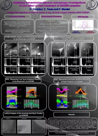
BiFeO3 Pt TiO2 Lim SiO2 Si 200 nm Example: Study of unknown phase in a BiFeO3 thin film Metal organic compound on Pt Heat treatment at 350oC (10 min) to remove organic parts. Process repeated three times before final heat treatment at 500-700 oC (20 min) . (intermetallic phase grown) Goal: BiFeO3 with space grupe: R3C and celle dimentions: a= 5.588 Å c=13.867 Å
27o 50 nm 15o 10o 0o Determination of the Bravais-lattice of an unknown crystalline phase Tilting series around common axis
0o 50 nm 19o 25o 40o 52o Determination of the Bravais-lattice of an unknown crystalline phase Tilting series around a dens row of reflections in the reciprocal space Positions of the reflections in the reciprocal space
011 111 001 101 6.04 Å 8.66 Å [101] [011] 7.94 Å 010 110 100 c b a Bravais-lattice and cell parameters [100] d = L λ / R From the tilt series we find that the unknown phase has a primitive orthorhombic Bravias-lattice with cell parameters: a= 6,04 Å, b= 7.94 Å og c=8.66 Å α= β= γ= 90o
O - K Fe - L2,3 BiFeO3 Ukjent fase 500 eV forskyvning, 1 eV pr. kanal Chemical analysis by use of EDS and EELS Ukjent fase BiFeO3 BiFe2O5
Published structure A.G. Tutov og V.N. Markin The x-ray structural analysis of the antiferromagnetic Bi2Fe4O9 and the isotypical combinations Bi2Ga4O9 and Bi2Al4O9 Izvestiya Akademii Nauk SSSR, Neorganicheskie Materialy (1970), 6, 2014-2017. Romgruppe: Pbam nr. 55, celleparametre: 7,94 Å, 8,44 Å, 6.01Å x y z Bi 4g 0,176 0,175 0 Fe 4h 0,349 0,333 0,5 Fe 4f 0 0,5 0,244 O 4g 0,14 0,435 0 O 8i 0,385 0,207 0,242 O 4h 0,133 0,427 0,5 O 2b 0 0 0,5 Celle parameters found with electron diffraction (a= 6,04 Å, b= 7.94 Å and c=8.66 Å) fits reasonably well with the previously published data for the Bi2Fe4O9 phase. The disagreement in the c-axis may be due to the fact that we have been studying a thin film grown on a crystalline substrate and is not a bulk sample. The conditions for reflections from the space group Pbam is in agreement with observations done with electron diffraction. Conclusion: The unknown phase has been identified as Bi2Fe4O9 with space group Pbam with cell parameters a= 6,04 Å, b= 7.94 Å and c=8.66 Å.