Download
1 / 35
420 likes | 632 Views
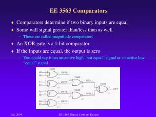
Comparators. A comparator compares two input words. The following slide shows a simple comparator which takes two inputs, A , and B , each of length 4 bits, and produces 1 if they are equal and a 0 if they are not equal.

E N D
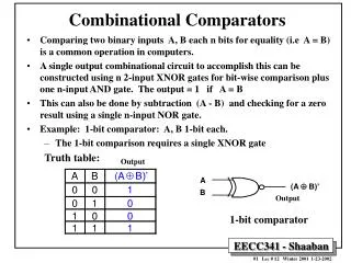
Comparators • A comparator compares two input words. • The following slide shows a simple comparator which takes two inputs, A, and B, each of length 4 bits, and produces 1 if they are equal and a 0 if they are not equal. • The circuit is based on the XOR gate (EXCLUSIVE OR) gate, which puts out a 0 if its inputs are equal and a 1 if they are unequal. • If the two words are equal, all four of the XOR gates must output 0. The results are then combined with a NOR gate.
Programmable Logic Arrays • Arbitrary functions (truth tables) can be constructed by computing product terms with AND gates and then ORing the products together. • A very general chip for forming the sums of products is the Programmable Logic Array or PLA. An example is shown on the following slide. • The user programs this array by burning out selected fuses (there are 1200 total fuses). The fuses burned determine which signals go to each AND gate.
Programmable Logic Arrays • The output consists of six OR gates, each of which has up to 50 inputs, corresponding to the 50 outputs of the AND gates. Once again a user supplied (50 x 6) matrix determines which connections actually exist. • A PLA can be used to compute the majority function described previously. Examine the diagram for the circuit. By using just 3 of the 12 PLA inputs, four of its 50 AND gates, and one of its six OR gates, we can implement the circuit. Actually, we could wire the PLA to compute simultaneously a total of four functions of similar complexity.
Programmable Logic Arrays • Field-programmable PLAs (shipped from the factories with all fuses intact and then programmed by the user) are still in use, but for many applications custom-made PLAs are preferable. • These are designed by the (large-volume) customer and fabricated by the manufacturer to the customer’s specifications. Such PLAs are cheaper than field-programmable ones. • We have seen three ways to compute the majority function.
Arithmetic Circuits • We now move from general-purpose MSI circuits to MSI combinatorial circuits used for doing arithmetic. • The first arithmetic MSI circuit we will examine is an eight-input, eight-output shifter. • Eight bits of input are presented on lines D0, … , D7. The output, which is just the input shifted 1 bit is available on lines S0, … , S7. The control line, C, determines the direction of the shift, 0 for left and 1 for right.
Adders • A hardware circuit for performing addition is an essential part of every CPU. The truth table for addition on 1-bit integers is shown on the next slide. • Two outputs are present: the sum of the inputs, A and B, and the carry to the next (leftward) position. • A circuit for computing both the sum bit and the carry bit is also shown on the next slide. • This simple circuit is generally known as a half adder.
Adders • A half adder is adequate for summing the low-order bits of two multiple input words, it will not do for a bit position in the middle of the word because it does not handle the carry into the position from the right. • For this, we need the full adder. A full adder is built up from two half adders. • Together the two half adders generate both the sum and the carry bits.
Adders • To build an adder for, say, two 16-bit words one just replicates the circuit 16 times. The carry out of a bit is used as the carry into its left neighbor. The carry into the rightmost bit is wired to 0. • This type of adder is called a ripple carry adder because in the worst case, adding 1 to 111 … 111 (binary), the addition cannot complete until the carry has rippled all the way from the rightmost bit to the leftmost bit. Adders without this delay are preferred.
Adders • Consider giving the adder two upper halves operating in parallel by duplicating the upper half’s hardware. Now instead of a single 32-bit adder, we have three 16-bit adders. • Call the upper halves U0 and U1. A 0 is fed into U0 as a carry and a 1 is fed into U1 as a carry. Now both start at the same time as the lower half starts, but only one will be correct. Select the correct one based on the lower half’s output. This is called a carry select adder. And the replication can be repeated.
Arithmetic Logic Units • Most computers contain a single circuit for performing the AND, OR, and sum of two machine words. Typically, such a circuit for n-bit words is built up of n identical circuits for the individual bit positions and is called an Arithmetic Logic Unit or ALU. • An ALU capable of computing A AND B, A OR B, B’, or A + B, depending on the function select lines F0 and F1 is shown on the following slide.
Arithmetic Logic Units • The lower left-hand corner of the ALU contains a 2-bit decoder to generate enable signals for the four operations, based on the control signals F0 and F1. Exactly one of the four enable lines is selected. • A or B can be forced to 0 by negating ENA or ENB, respectively. It is also possible to get A’, by setting INVA. Under normal conditions, ENA and ENB are both 1 to enable both inputs and INVA is 0. We will later see uses for INVA, ENA, and ENB.
Arithmetic Logic Units • The lower right-hand corner of the ALU contains a full adder for computing the sum of A and B, including handling the carries, because it is likely that several of these circuits will eventually be wired together to perform full-word operations. • Circuits like the one shown are actually available and are known as bit slices. They allow the computer designer to build an ALU of any desired width.
Clocks • In many digital circuits the order in which events happen is critical. • To allow designers to achieve the required timing relations, many digital circuits use clocks to provide synchronization. • A clock is a circuit that emits a series of pulses with a precise pulse width and precise interval between consecutive pulses. • The time interval between the corresponding edges of two consecutive pulses is known as the clock cycle time.
Clocks • Pulse frequencies are commonly between 100 MHz and 4 GHz, corresponding to clock cycles of 10 nsec to 250 psec. • To achieve high accuracy, the clock frequency is usually controlled by a crystal oscillator. • In a computer, many events may occur during a single clock cycle. If these events must occur in a certain order, the clock cycle must be divided into subcycles. A secondary clock signal phase-shifted from the primary may be generated with a delay circuit.
Clocks • The four time references are: • Rising edge of C1 • Falling edge of C1 • Rising edge of C2 • Falling edge of C2 • By tying different events to the various edges, the required sequencing can be achieved. If more than four time references are needed, more secondary lines can be tapped from the primary, with different delays.
Memory • Memory is an essential component of every computer. We will now see the basic components of a memory system starting at the gate level. • To create a 1-bit memory, we need a circuit that remembers previous input values. Such a circuit can be constructed from two NOR gates. Analogous circuits can be built from NAND gates.
Latches • The circuit on the next slide is called an SR latch. • It has two inputs, S, for Setting the latch and R, for Resetting it. • It also has two outputs, Q and Q’, which are complementary. • Unlike a combinatorial circuit, the outputs of the latch are not uniquely determined by the current inputs. • Assume that both S and R are 0. Assume that Q = 0. Because Q is fed back into the upper NOR gate, both of its inputs are 0, so its output is 1.
Latches • Now imagine that Q is not 0 but 1, with R and S still 0. The upper gate has inputs of 0 and 1, and an output of 0, which is fed back to the lower gate. • A state with both outputs equal to 0 is inconsistent, because it forces both gates to have two 0s as input, which, if true, would produce 1, not 0, as output. • Similarly, it is impossible to have both outputs equal to 1. • The conclusion: for R = S = 0, the latch has two stable states, which we will refer to as 0 and 1, depending on Q.
Latches • Now examine the effect of the inputs on the state of the latch. Suppose that S becomes 1 while Q = 0. The inputs to the upper gate are then 1 and 0, forcing the Q’ output to 0. This change makes both inputs to the lower gate 0, forcing the output to 1. • Thus, setting S switches the state from 0 to 1. • Setting R to 1 when the latch is in state 0 has no effect. • Setting S to 1 when in state Q = 1 has no effect, but setting R drives the latch to state Q = 0. • The circuit “remembers” whether S or R was last on.
Latches • It is often convenient to prevent the latch from changing state except at certain specified times. • The circuit to accomplish this is called a clocked SR latch. • The circuit has an additional input, the clock, which is normally 0. With the clock 0, both AND gates output 0, and the latch does not change state. When the clock is 1, the latch becomes sensitive to S and R. The terms enable and strobe mean that clock input is 1.
Latches • When both S and R are 1, the circuit becomes nondeterministic. • A variant, the clocked D latch prevents the situation from occurring
Flip-Flops • It is generally preferable to allow the state of the circuit to change only at particular instants of time • Latches can change as long as the clock value is 1 (level triggered) • Flip-flops can change state only on the clock transition from 0 to 1 or 1 to 0 (edge triggered) • Use a pulse generator with a very short pulse