Download
1 / 47
470 likes | 574 Views
Forward Vertex Detector Status: R&D: Scientific and Technical Resources. Technical Design Overview Design status R&D Cost and schedule Scientific Resources and Manpower Issues and Concerns. Forward Vertex Detector Technical Design – Specifications.

E N D
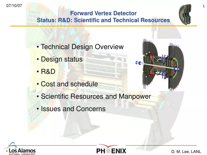
Forward Vertex DetectorStatus: R&D: Scientific and Technical Resources • Technical Design Overview • Design status • R&D • Cost and schedule • Scientific Resources and Manpower • Issues and Concerns
Forward Vertex DetectorTechnical Design – Specifications • Cover the Muon Spectrometer Acceptance – both Arms (10-35 deg) • Full Azimuthal coverage – hermetic • DCA resolution < 200 µm at 5 GeV • ≥ 3 space points / track • Maximum Radiation Length < 2.4% • Survive 10 year integrated dose = 200k Rad • Low Occupancy in Au – Au Central < 10.0% • Co-exist with barrel VTX • Compatible with PHENIX DAQ
Forward Vertex DetectorTechnical Design – Mechanical “Big Wheel” Location for all readout electronics Combined VTX + FVTX without outer enclosure FVTX
Forward Vertex DetectorTechnical Design – Mechanical Each Endcap 4 hermetic disks, z=18.5 – 38 cm 48 wedge segments per disk ( 7.5 deg) Inner disk radius = 3.5 cm (4.5 cm active) Outer disk radius = 17 cm 75 micron strips, 550,000 strips/endcap Total power load of disks = 50 W each Power load of Readout cards= 450 W in big wheel Room temperature operation
Forward Vertex DetectorTechnical Design – Mechanical Mechanical Integration with the Barrel VTX Fully integrated model
Backplane HDI Detector FPHX Chips Rigid, thermally conductive epoxy Rigid epoxy Forward Vertex DetectorTechnical Design – Wedge Connectors for extension cables Screw (nylon) HDI Pin hole (for alignment) Detector FPIX Chips (26, 13 ea. side) Backplane (0.76mm graphite fiber composite) All bonded with rigid epoxies Screw (nylon) Pin hole (for alignment)
HDI Sensor HDI FPHX Chips (13 per column) Forward Vertex DetectorFVTX Sensor • Sensor • 2 columns of strips • 1664 strips per column • strip length 2.8 to 11.2 mm • 75 µm spacing • 48 wedges per disk (7.5˚/sensor, ~15˚/wedge) • 0.5 mm overlap with adjacent wedges • FPHX Chip • 1 column readout • 128 channels • ~ 70 µm channel spacing • Dimensions –9mm x 1.2 mm Mini-strips are oriented to approximate an arc
Sensor layoutR&D prototyping design Zoom in … one FPHX chip Thickness 300 µm Doping of starting material n type Resistivity 2-5 K-cm Wafer diameter 6 “ preferred Passivation SiO or SiN bonding pads testing pads (both staged) Guard ring Vaclav Vrba, Prague Dicing edge
SensorR&D A real prototype Vaclav Vrba, Prague
HDI Stack Up GND Signal Signal Power Forward Vertex DetectorHDI-High Density Interconnect kapton • High Density Interconnect (HDI) – kapton flat cable to transfer data from the chip to the read-out electronics • 176 μm thick • 4 copper planes (ground, power, 2ea signal), 5 Kapton films, 8 glue layers glue glue kapton glue glue kapton glue glue kapton glue glue kapton HDI • HDI trace count • 2 R/O lines x LVDS pair x 26 chips 104 • 4 Download and Reset lines 4 • 2 Clocks x LVDS pair 4 • 1 Calibration line 1 • 113
Wedge R&D AnalysisTemperature & Stress Max deflection 10.4μm • Warmest FPHX Chip is 5.3ºC Warmer than Back Edge of Backplane Min Tº = 15ºC Max Tº = 20.3ºC Warmest ROC Zero deflection (boundary conditions) 3-D Temperature Contour 3-D Distortion Contour
Single piece plastic insert for screws and pins Standoff plate Thermally conductive Silicone Foam core Honeycomb core Plastic inserts for screws and pins Forward Vertex DetectorHalf-Disk Assembly: Details
Max deflection of detector ~8μm Disk-Level R&D Modeling Thermal distortion Distortion due to cooling Fundamental vibration mode: 164 Hz
Cooling hose (silicone) Station 1 Station 2 Station 3 Station 4 Half Cage Assembly Y Al Honeycomb core, C face sheets Z
Liquid Cooling CircuitR&D Outlet plane 4: 10.3°C Outlet plane 2: 10.9°C station 2: ~21.2°C station 4: ~20.6°C Warmest Chip, station 1: ~21.4°C FVTX Outlet: 11.1°C, ~3 psig station 3: ~20.9°C FVTX Inlet: 10°C, ~5 psig Outlet plane 3: 10.6°C
Half Cage AssemblyR&D Drum mode shape (f=137.7 Hz) Gravity Sag (Max = 3.2µm)
VTX+FVTXFinite Element Model R&D First Mode: 38Hz
Data Word structure TBD FPHX Chip DesignR&D Phase 1 • Designed by FNAL • Based upon well tested FPIX2 chip design • Data push readout over 2 output lines • Zero suppression with programmable threshold • Fully programmable logic with masking capabilities • Data contains: • 3 bit ADC • 7 bit Strip Information • 6 bit Beam Counter • Noise 150e + 140e/pf • Power <110 µW per channel Time (ns)
FPHX Chip DesignSpecifications – Phase 2 • Match to 75 µm strip spacing, ~ 70 µm channel spacing • Design to strip capacitance ≤ 1.5 pf • Dynamic range to extend to 50000 e- • Noise ≤ 425 e- • Chip readout, 4 hits in 4 beam clocks • Use Data push architecture • 4 bit ADC required, 5 bit goal, with programmable reference voltages • 2 output lines • All other FPIX2 specifications* • * FPIX2 has same output architecture as FPHX so FPIX2 is used for testing DAQ designs
Forward Vertex DetectorTechnical Design – Electronics DAQ Readout electronics split into two parts • Near the detector (ROC) • Compresses and serializes the data from a group of chips • Radiation tolerance use FLASH based FPGAs from Actel • Fiber link to the control room • In the Control Room (FEM) • Buffer data for 64 beam clocks • Send data to DCM upon LVL1 trigger request • SRAM based FPGAs from Xilinx LVL1 GTM Slow Control 2.5 Gb/s fiber link fiber N FPHX Chips FEM PHENIX DCM ROC 1,2 output lines per chip Stream of 20-bit data words @ 150 MHz– under design Zero suppression Programmable Threshold Deserialize and Combine data from several FPHX chips Strip Synch Words Send data over fiber Calibration Buffers Data for 64 Clocks Upon Lvl-1 grab relevant data Build packet Send data to DCM/LVL1 Pass Clock to ROC Slow controls manager PHENIX Standard Limit <2000 20-bit words/DCM Inside IR In Counting House
ROC Design Specifications • Combine serial data from 52 FPHX chips ( 2 wedges) • Synchronize readout and strip off Sync Words • Generate ~130 MHz Serializer Clock • Provides Control, Download and Calibration signals for the chips • Append CHIP ID to the data • Send parallel data word output at 130 MHz over 2 fiber interface to the FEM • Move from ACTEL A3PE600 to ACTEL A3PE3000 FLASH based FPGA = done
8-chip module USB Interface DigiIO Actel Board ROC Prototype R&D • Actel A3PE600 prototype board • Slow control via USB interface (DLP-2232M) • Output data via NI-6534 PCI card at 20 MHz (up to 640 Mbps) • Test an 8-chip FPIX module (FPIX is progenitor of FPHX chip and has similar digital backend)
8-chip module USB Interface DigiIO Actel Board ROC Prototype R&D Covers 30 deg (16 wedges)
FEM Design Specifications • FEM receives data from a single ROC channel over two fibers at fixed rate of 2.5 Gbits/s • Main functionality • Store the data by BCO counter • Buffer data for 64 BCO clocks • Read the data from certain clock to output buffer at 300 MHz • Send the output buffer content to the DCM • Plan to combine the data from 4 FEM channels on single FEM board • Implementation • Xilinx mid-scale Virtex-4 FPGA VC4VSX35 • Use built-in FIFOs and Relationally Placed Macros (RPMs) for maximum performance and predictability (Provided by XILINX) = done
FEM R&D • Design tested with single chip readout and “fake” data and running chip calibration chain • 100% of hits propagates through FEM with realistic triggered readout • Readout to PC tested at 640 Mb/s rate using NI-6534 readout board Virtex-4 test board FPIX Chip
Test of Calibration System • Test each pixel by injecting 64 pulses at gradually increasing amplitude • Upper figure shows histogram of turn-on curve for one channel • Lower figure shows noise • Inject capacitor = 3fF Noise ~ 102 e
Summary Designs and R&D • Mechanical design is well along and mature • Some mechanical prototyping needed • Sensor prototype finished and ready for testing • Readout ROC and FEM prototyped and tested • Fiber link prototyped and under test • All other requirements met • Calibration circuit designed and to be implemented on ROC board • FPHX conceptual design done, first pass • FPHX R&D critical path FEM with fiber readout
Remaining R&D • DAQ – ROC and FEM electronics PC boards are now in progress and will be complete by Jan 2008 – LDRD funded • FPHX – complete design and chip layout – SOW in progress, signed by LANL and FNAL, ready for BNL signature – Start July 2007 • FPHX – First MOSIS run, early 2008 • Mechanics – some prototyping desirable 2007 FEM with fiber readout
Cost Basis - Major Items Mechanical structures – HYTEC estimate based on prior experience with VTX and ATLAS Sensors – Quotes from CIS, MICRON FPHX – FNAL estimate based on prior experience Electronics Interface DAQ – estimate based on prior experience Wire bonding – PROMEX quote DCM,slow controls, etc – Muon system experience, Steve Boose
FVTX Schedule Assumptions • Construction start – January 1, 2008 ( 2nd QTR FY08) • LANL R&D start - January 2006 • BNL R&D start – October 2006 • Schedule durations determined by engineering estimates, vendor quotes • Duration of project made to match funding profile • VTX and LDRD impact the schedule especially R&D • Wedge assemblies tested at a rate of 3/day ( automated computer tests) • Disk assembly assembled in 2 week, metrology of disk in 2 week • Commissioning for 8 months
FVTX Major Cost Items Major Item Base Cost Contingency Sum Mechanical Ladder and support $416k 26% $524k Sensor $410k 26% $517k FPHX Chip $240k 36% $326k Wire bonding $188k 26% $237k ROC board s $443k 36% $603k FEM boards $323k 36% $440k HDI $111k 25% $139k Total Project (FY07) $3669k 25% $4595k
Scientific resources and Manpower 7-2-2007 Draft
Infrastructure and Facilities • Columbia – Electronics lab and test equipment, 400 sq ft clean room • Czech – Electronics lab and test equipment, clean room • LANL – Electronics lab and test equipment, 600 sq ft clean room • UNM – 256 sq ft clean room, probe station, test equipment • BNL – lab space, measurement facilities UNM Clean Room Columbia Clean Room LANL Clean Room
Issues and Concerns • FPHX is new and the highest risk item – will require careful attention • Integration – VTX/FVTX integration • Strip layers still being designed • Big wheel electronics • Electrical – grounding and shielding • Extensive system tests will be required
R&D Costs Associated for FVTX • LANL LDRD-DR - $589.9k expected ( to date) finish • DAQ Interface Modules - $489.9k ($100.9k) Jan2008 • Mechanical design - $100k ($100k) Apr2007 • LANL Heavy Ion Program - $130k • Mechanical design - $130k ($130k) Apr2007 • BNL R&D funds - $345k • FPHX design and Prototype - $295k ( $67k) Jul2008 • Mechanical prototype - $50k ($0k) Jan2008 • Czech Institute of Physics, Academy of Sciences • Sensor – prototype finished – contribution
VTX – FVTX IntegrationThe need began 2 years agoBut we found this 2 months ago Interference!
Manpower Fraction 35% 65%