Download
1 / 23
240 likes | 351 Views
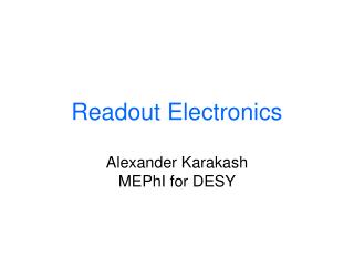
MTD Readout Electronics. J. Schambach University of Texas Hefei, March 2011. TOF Electronics Overview. The same as TOF, mostly…. THUB , TCPU , TDIG are identical Each TCPU reads out 3 or 5 TDIG (1 backleg ) MINO is a 4- NINO version of TINO

E N D
MTD Readout Electronics J. Schambach University of Texas Hefei, March 2011
The same as TOF, mostly… • THUB, TCPU, TDIG are identical • Each TCPU reads out 3 or 5 TDIG (1 backleg) • MINO is a 4-NINO version of TINO • Each MTD tray gets 1 MINO & 1 TDIG • MTRG – this is a new card; it combines the NINO trigger outputs logically and sends a signal to trigger: the earliest east-end and west-end signal for each backleg • MFTB – a new un-powered board that “closes” the gas box (tray) and passes the MRPC signals to MINO • There are 2 THUB, 28 TCPU, 118 TDIG, 118 MINO, and 28MTRG boards in the MTD electronics
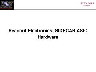
Large dynamic range Hit FIFO orDual port RAM Trigger Triggertime tag Latency - Compare time Output FIFO HPTDC: Data driven TDC • Only stores data when hit detected • Variable latency over full (1/4) dynamic rangeCompromise between hit rate and latency • Triggered / non triggered mode • Multiple overlapping triggers • Channel merging possible via derandomizersLimits hit rates • Good double pulse resolutionBut complicated dead time analysis • Buffer occupancies must be seriously analyzed • Buffer overflows must be handled carefully • Hit may be lost if marked • Complete events must never be lost • Wide latency buffer (covers full dynamic range) • More complicated architecture/implementationPrevious data driven TDC worked well in different applications • Logic complication handled by logic synthesis • Extended verifications at behavioral/register/gate level • High flexibility Derandomizer FIFO’s Common FIFO
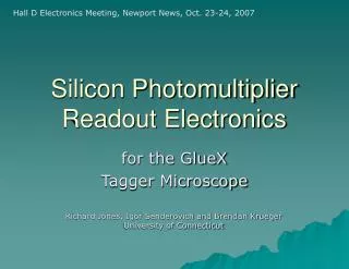
LSB MSB Coarse time(bin width 25 ns, 11 bits) PLL bits (bin width 3.125 ns) DLL bits (bin width 98 ps) R-C bits (bin width 24.4 ps) HPTDC Time Measurement HPTDC is fed by a 40 MHz clock giving us a basic 25 ns period (coarse count). A PLL (Phase Locked Loop) deviceinside the chip does clock multiplication by a factor 8 (3 bits) to 320 MHz (3.125 ns period) . ADLL (Delay Locked Loop) done by 32 cells fed by the PLL clock acts as a 5 bit hit register for each PLL clock (98 ps width LSB = 3.125 ns/32). 4R-C delay lines divide each DLL bin in 4 parts (R-C interpolation)
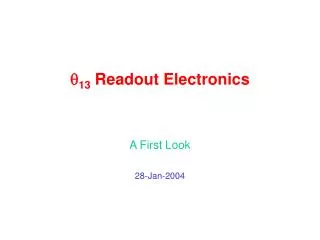
HPTDC Buffering & Readout 8 channel @ 25ps or 32 channels @ 100ps Level-0 Trigger Bunch Crossing Hit Buffer Level-0 Buffering
DAQ/Trigger Interface THUB National’s SerDes Chip
Source Interface Unit Destination Interface Unit ALICE DDL Link Front-end electronics DDL SIU Detector Data Link Optical Fibre ~200 meters DDL DIU Read Out Receiver Card RORC PCI PC Data Acquisition PC J. Schambach
THUB J. Schambach
Electronics Monitoring & Configuration Tool J. Schambach