Download
1 / 11
110 likes | 249 Views
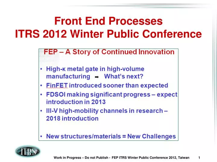
Front End Processes ITRS 2012 Winter Public Conference. 2012 ITRS FEP Sub-TWG Leadership. HP MPU ASIC (Table FEP 2) Wei-Yip Loh (US) LOP (FEP 3) Wei-Yip Loh (US) LSTP (FEP 4) Wei-Yip Loh (US) DRAM (FEP 5) Ho Jin Cho (KR) Floating Gate Flash (FEP 6) Mauro Alessandri (EU)

E N D
2012 ITRS FEP Sub-TWG Leadership • HP MPU ASIC (Table FEP 2) • Wei-Yip Loh (US) • LOP (FEP 3) • Wei-Yip Loh (US) • LSTP (FEP 4) • Wei-Yip Loh (US) • DRAM (FEP 5) • Ho Jin Cho (KR) • Floating Gate Flash (FEP 6) • Mauro Alessandri (EU) • Charge Trapping Flash (FEP 7) • Mauro Alessandri (EU) • PCM (FEP 8) • Mauro Alessandri (EU) • FeRAM (FEP 9) • Yukinobu Hikosaka (JP) • Starting Materials (FEP 10) • Mike Walden (US) • Mike Goldstein (US) • Surface Preparation (FEP 11) • Joel Barnett (US) • Therm/Thin Films/Doping (FEP 12) • Wei-Yip Loh (US) • Etch (FEP 13) • Tom Lii (US) • CMP (FEP 14) • Darryl Peters (US)
+ III/V and Ge High µAlternative Channel Mat’ls New Structures and Materials for Transistors and Memory Next Generation Metal Gate/High-k Stacks New High Mobility Channel Materials Advanced Memory 3D Devices - Formation, Doping, Stress FDSOI New Memory Materials Phase Change Memory
FEP Difficult ChallengesNear Term • Sustaining Strain Engineering - Continued effective use for increasing device performance - Application to FDSOI and Multi-gate technologies • Achieving DRAM Cell Capacitance with Dimensional Scaling - Discovering robust dielectric with dielectric constant of ~60 - Finding electrode material with high work function • Realizing Clean Surfaces Free of Killer Defects - No resultant pattern damage - Very low material loss (<0.1 A) • Broad Adoption of High-k/Metal Gate - Introduction to full scale manufacturing for HP, LOP, and LSTP • Application to advanced structures and materials - Scaling equivalent oxide thickness (EOT) below 0.8nm while maintaining acceptable electrical performance • 450mm wafers - production level quantities at advanced technology generations anticipated for roadmap intersection
FEP Difficult ChallengesLong Term • Continued scaling of HP multigate device in all aspects: EOT, junctions, mobility enhancement, new channel materials, parasitic series resistance, contact silicidation. • Lowering required DRAM capacitance by 4F2 cell scheme or like, while continuing to address materials’ challenges • Continued achievement of clean surfaces while eliminating material loss and surface damage and sub-critical dimension particle defects • Continued EOT scaling below 0.7 nm with appropriate metal gates • Continued charge retention with dimensional scaling and introduction of new non-charged based NVM technologies
2012 Logic Update • New metrology requirements considered • USJ, 3D and new channel materials • Establishing criteria for deciding how new technology's will be incorporated as tables • Interaction with PIDS to address: • Vdd and FDSOI pull-in • n-III-V and p-Ge table entries
2012 FeRAM Update Worked with PIDS to better align the two TWGs’ FeRAM-related 2011 tables
2012 Starting Materials Update • Continued to monitor industry activities related to 450mm development and assess impact on the Starting Materials table entries • Addressed wafer flatness colorization issues • Ongoing review of progress relative to FinFET (SOI-based) adoption and consideration to revisit SOI starting layer thickness table entries, as appropriate
2012/2013 Surface Prep Update • Critical particle size driver. ½ DRAM half pitch is current driver but flash is smaller • Modifying specification for AFM measurement of roughness to reflect decreased critical area size • Address the difficult aspects of measuring low-k value due to damage/failure • Address ESH aspects of III-V cleans (generation of phosphine, arsine gases) • Include anti-stiction drying for pattern collapse in Potential Solutions table (typically a MEMS issue)
2012 Etch Update • Gate CD variation updates • With grid design rule widely used at gate layer, through pitch Lgate variation item is removed from total gate CD variation calculation • Replacement gate high-K last dummy gate stack removal induced Lgate variation was added into total gate CD variation calculation • Advanced gate etch chamber clean helped to improve wafer to wafer and lot to lot Lgate variations • Gate LWR performance is marginal from 2012 LWR becomes largest portion of gate CD variation. High power plasma UV resist treatment is a potential LWR improvement method
2012 CMP Update Addressed replacement metal gate (RMG) Obtained metrics from end users for RMG (Poly-open Process and metal polish) Revised RMG table Added text for RMG post-CMP cleans Revised challenges