Download
1 / 23
250 likes | 472 Views
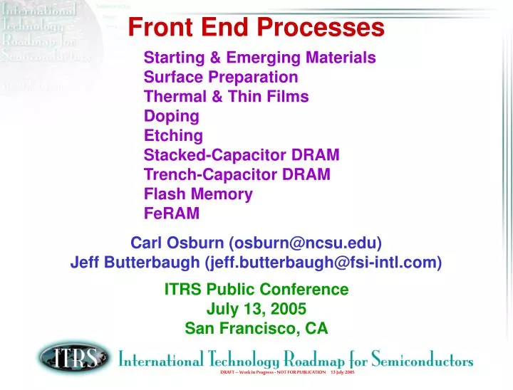
Front End Processes. Starting & Emerging Materials Surface Preparation Thermal & Thin Films Doping Etching Stacked-Capacitor DRAM Trench-Capacitor DRAM Flash Memory FeRAM. Carl Osburn (osburn@ncsu.edu) Jeff Butterbaugh (jeff.butterbaugh@fsi-intl.com). ITRS Public Conference

E N D
Front End Processes Starting & Emerging Materials Surface Preparation Thermal & Thin Films Doping Etching Stacked-Capacitor DRAM Trench-Capacitor DRAM Flash Memory FeRAM Carl Osburn (osburn@ncsu.edu) Jeff Butterbaugh (jeff.butterbaugh@fsi-intl.com) ITRS Public Conference July 13, 2005 San Francisco, CA
Starting Materials – Defect Densities Issues and Challenges • HP MPU chip size • Previous ITRS defect densities were based on C/P chip sizes (~140 mm2) • Allowable defect densities for HP MPU consider new chip size scenario in 2005 • Site Flatness and Nanotopography • SFQR remains the most commonly used metric • Lack of consensus regarding requirement • some IDM’s favor values greater than the technology generation (TG) while others state values equal to or less than TG • Nanotopography impact is not universal, seemingly critical for some IDM’s but of little interest to others
Starting Materials-Edge Exclusion • Set at 1.5 mm in 2007 (from 2 mm in 2003) by Factory Integration TWG, Where it will be Red • Implementation Poses a Significant, Immediate Challenge in FEP • Edge Rolloff • Definition currently being addressed by SEMI / JEITA • Assessment of table entry for future ITRS publications (post 2005) to be implemented once agreed upon metric is obtained • Defects • Leading, Current SOI Manufacturing Processes Produce a Spatial Region that is not Usable Real Estate for IC Production – Hence Coloration Starts with Red
Emerging Materials Ultra-Thin Body, Fully-Depleted SOI • Layer Thicknesses Reduced Based Upon More Thorough PIDS Designs • 0.35 x Lgate = 8 nm +/-10% in 2008 Strained Silicon and Strained Silicon on Insulator (sSOI) • Treated in Starting Material’s Sub-chapter Text Orientation Modification for Optimization of CMOS Electron and Hole Mobility Values • Treated in Starting Material’s Sub-chapter Text
450 mm Wafers • 450 mm Wafers Required in 2012 (per ORTC direction) • Introduction of 450 mm presents unprecedented challenges • Technical (meeting specs over larger areas) • Economic (especially for wafer, equipment, and metrology suppliers) • Critical path definition - We are already late to meet this development cycle • Standardization • Wafer specification (type, thickness, diameter tolerance, etc.) • Factory automation (load lock, transportation method, etc.) • Wafer package (FOSB, FOUP, door configuration, etc.) • 450 mm Wafer Issues Will be Highlighted in 2005 ITRS • FEP subchapter on this topic • Supplemental position paper • Inclusion of material in executive summary
Yield Model and Surface Particles • Killer defect density value for Surface Prep is calculated based on Poisson’s model for yield = 99% • Values changes from 2004 are small, due to die size changes • 97 (in 2004 ITRS) to 94.2 (in 2005 ITRS) for 2005 critical particle count per wafer • Currently different models are used for Yield Enhancement and Starting Materials/ Surface Prep • Final particle density values are approximately the same for all models, however use of different equations is because goals of groups are different • YE and FEP will have a workshop to determine the appropriate Starting Materials’ defect levels and establish specific call outs for critical cleans (specifically pre-gate) • Concern is ability to measure defects at critical particle diameter that contributes to yield loss
Back Surface and Edge Particles • Goal for 2005 is to relate back surface particles to yield • Currently little public data available to set metrics • The values in the 2004 and 2005 are based on survey results • 2005 ITRS value are the same as the 2004 update • Wide range of data obtained in the survey • Survey results are not consistent Yield Model • Contribution from edge particles will be examined in 2005/6 • Contribution from cluster of back surface particles vs. single particles are known to be important • Especially to Lithography depth of focus
Other Surface Prep Changes • Watermark criteria re-established at table metric • Watermark = 0 for all years • Silicon and oxide loss numbers continually decrease, down to 0.4Å at 57 nm node, and 0.2Å at 32nm node • Inclusion of discussion of high-k and the surface preparation requirements • Gate oxide dielectric and high-k have same low contamination requirements • Values With No Changes in 2005 • Critical GOI metals and mobile ions • Surface Roughness • Surface carbon contamination
Parallel Lines to Capture Alternative Device Scenarios • Extended Bulk and PD-SOI Devices to Overlap 4 Years with FD-SOI / Multi-Gate • Recognizes Different Approaches in Different Companies • Roadmap will Illustrate Requirements for Different Scenarios • Increases the Number of Lines in the Table • FD-SOI and multi-gate will be placed on separate, over-lapping lines. 2005 2006 2007 2008 2009 2010 2011 2012 2013 2014 2015 2016 Bulk/PD-SOI FD-SOI Multi-Gate The Baseline Scenario Envisions a Nominal Switch from Bulk to FD-SOI Around 2008, and a Switch to Multi-Gate Around 2012
Deferred Implementation of High k Year2003 ITRS2005 ITRS 2004 2005 2006 2007 2008 Enhanced Mobility “ “ High k for Low Power High K for MPU Metal Gate FD-SOI Enhanced Mobility High k for Low Power High K for MPU Metal Gate FD-SOI • Puts Multiple, Major Changes into One Year (2008) • Causes Other Parameters, e.g., Xj, to Scale More Aggressively
Metal Gate Electrode Work Functions • Constraint was Added to PIDS Device Design Scenario for Bulk, FDSOI, and Multi-Gate, Namely to Minimize the Number of Different Work Function Metals Needed Over Time • Three-Four Systems Seen to Meet All Needs Through 2020 • Band Edge (~100 meV inside band) for Bulk • ~150 meV Above*/Below* Midgap for HP FDSOI • Midgap for HP Multi-Gate, LOP FDSOI and Multi-Gate • ~100 meV Below*/Above* Midgap for LSTP FDSOI and Multi-Gate • Improvements Can be Made by Allowing Workfunction to Vary Yearly, but fms Control is a Vt Tolerance Issue • Band Edge Metal Gates Viewed as Limiting Factor in High k Deployment NMOS*/PMOS*
Doping and Junctions • EOT Values to be Given for Different Poly-Si Doping Levels • 1e20/cm3 (lightly-doped) tdepletion ~ 0.5 nm • 1.5e20/cm3 (baseline doping) tdepletion ~ 0.4 nm • 3e20/cm3 (advanced, e.g., laser annealed) tdepletion ~ 0.2nm • Junction Depths are Scaled More Aggressively in 2005 to • Accommodate Slower EOT Scaling • Junction Implant Parameters to meet Xj-Rs Requirements to • be Given in Supplemental Tables • Maximum Implant Energy • Dose • Series Resistance Becomes a Increasingly Important • Limitation (Ominous) • Scenario, Rather than Requirements, Given for Elevated • Junctions in FDSOI and Multi-Gate
Repartitioning of Lithography and Etch Contributions to Physical Gate Length • Issue: Neither Etch nor Lithography Could Meet Tolerance Budgets to Achieve +/- 10% Control of Physical Gate Length • 2005 “Partial Solution”: • Maintain Final (Etched) Physical Gate Length at 2003 Values • Relax (increase) Printed Gate Length Dimension in Resist • Increase the Amount of Resist Trim • Increase the Total Tolerance on Physical Gate Length to 12% • Repartition Tolerance Budgets from 80% Litho/20% Etch to • 75% Litho/25% Etch Observation: At the “90 nm Node”, Most Manufacturers are using Gate Lengths Longer than ITRS Values. - If Trend Persists, ITRS Values May Need to be Adjusted Upwards
Gate Etching • Gate sizing variation allowance • Surveys in 2003 and 2004 indicated that the industry • was not processing etched gates at <10% 3 sigma • Feedback from device modeling indicated that relaxing • to 12% 3 sigma would not degrade performance • Requirements for gate etch were relaxed as follows: (Litho is given 75% of the allowable gate length variance)
Gate Etching Increase of overall gate sizing tolerance from 10-12% and allocation of variance to etch from 20-25% - Increases Litho allowance by 18% - Increases Etch allowance by 35% - Allows improved coloration of the table entries 2001 ITRS 2003 ITRS 2005 ITRS
Stacked-Capacitor DRAM Changes for ITRS 2005 Cell size factor, a, is projected to remain at 8 through 2007—not scaling as rapidly as projected in 2003-4 Capacitor dielectric material and Dielectric constant are modified based on survey of DRAM manufacturers
Modified Parameters for Stacked-Capacitor DRAM Capacitor dielectric material new material ALO /TAO ALO /TAO /others ALO/TAO TIO /new material ALO /(A)HO ALO /TAO /(A)HO new material ALO/TAO /AHO ALO /HO STO/new material Proposal for 2005 100 22 40 50 50 50 50 50 60 60 60 80 80 80 100 100 100 Dielectric constant Year of Production 16 17 18 19 20 04 05 06 07 08 09 10 11 12 13 14 15 8.0 7.5 7 7 6 6 6 6 6 6 6 6 6 5 5 Cell size factor a 8 8 8 6 6 6 6 6 6 6 6 6 6 6 6 6 Proposal for 2005 - Discussions still on-going regarding capacitor dielectric material
Trench-Capacitor DRAM Roadmap Bottle Geometry HSG Aspect Ratio 60:1 >100:1 Effective Oxide Thickness 5.2nm 1.2nm Materials High-k Dielectric Metal Electrode New materials
Trench-Capacitor DRAM RoadmapChanges in 2005 versus 2004 Update Solutions exist down to 57nm node (WAS: 70nm)“Red brick wall” moved out to 28nmHigher trench aspect ratios anticipated for ≤ 45nm MIM option for ≤ 50nm (WAS: ≤ 45nm)MIM only option for ≤ 35nm (WAS: epi-high-k as 2nd option)
ITRS 2005 Trench DRAM Roadmap Known Solutions exist through 57nm node “Red brick wall” moved to 28nmMIM option for ≤ 50nm; only option for ≤ 35nm
Flash Memory Poly 2 Poly 2 Poly 2 Poly 2 45 nm 65 nm Decoupling IPD IPD IPD IPD Poly 2 50-60 nm 60-80 nm Poly 1 Poly 1 Poly 1 Poly 1 IPD • A sharp decrease in the interpoly dielectric (IPD) EOT is needed at 45-50 nm, for NOR, and maybe for NAND, to enable further scaling of the Bit Line pitch and the Floating Gate spacing and to maintain an acceptable Coupling Ratio (CR) 10-12 nm EOT 4-6 nm EOT • ONO (Oxide-Nitride-Oxide) technology is no longer feasible and new materials/architecture are necessary (e.g., high-k,…) • Alternatively new floating gate design (e.g., SiN charge storage) • Since STI may be formed post floating gate and because it is deeper, its aspect ratio is higher than in logic trench fill technology is more critical (MLD or SOD)
FeRAM Roadmap • Japan PIDS Surveyed the Commercial Production Status of FeRAM • 2005 Technology Node Feature Sizes will be for Stand-alone memory at 10k/mo volume by 2 companies (as with DRAM) • 2003-4 ITRS Used Both Stand-alone and Embedded Memory • Scaling Rate of FeRAM is Subject of Ongoing FEP/PIDS Discussion
FeRAM Roadmap • Access and Cycle Time are now Expected to Scale More Slowly than Projected in 2003 ITRS • Assuming a Minimum Switching Charge Density of 30mC/cm2 and a Bit Line Voltage Swing of 140mV, 3 Dimensional (3D) Capacitors will be Needed in 2010 • Definition of Minimum Switching Charge Density after 3D Introduction will be Determined with PIDS