Download
1 / 15
150 likes | 513 Views
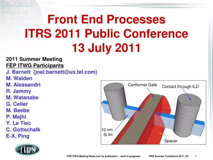
Front End Processes ITRS 2011 Public Conference 13 July 2011. Conformal Gate. Contact through ILD. 2011 Summer Meeting FEP ITWG Participants J. Barnett (joel.barnett@us.tel.com) M. Walden M. Alessandri R. Jammy M. Watanabe G. Celler M. Beebe P. Majhi Y. Le Tiec C. Gottschalk

E N D
Front End ProcessesITRS 2011 Public Conference13 July 2011 Conformal Gate Contact through ILD 2011 Summer Meeting FEP ITWG Participants J. Barnett (joel.barnett@us.tel.com) M. Walden M. Alessandri R. Jammy M. Watanabe G. Celler M. Beebe P. Majhi Y. Le Tiec C. Gottschalk E-X. Ping 10 nm Si fin Slide 1 Spacer
2011 ITRS FEP Sub-TWG Leadership • HP MPU ASIC - FEP 2 • Prashant Majhi (US) • LOP - FEP 3 • Prashant Majhi (US) • LSTP - FEP 4 • Prashant Majhi (US) • DRAM - FEP 5 • Deok-Sin Kil (KR) • Floating Gate Flash - FEP 6 • Mauro Alessandri (EU) • Charge Trapping Flash - FEP 7 • Mauro Alessandri (EU) • PCM - FEP 8 • Mauro Alessandri (EU) • FeRAM - FEP 9 • Yoshimasa Horii (JP) • Starting Materials - FEP 10 • Mike Walden (US) • Mike Goldstein (US) • Surface Preparation - FEP 11 • Joel Barnett (US) • Therm/Thin Films/Doping - FEP 12 • Prashant Majhi (US) • Etch - FEP 13 • Tom Lii (US) • CMP - FEP 14 • Darryl Peters (US)
FEP 2011 one-page Summary • Memory: Continue NOR Flash at least to 22nm; keep PCM in table with minor update; define 3D CT critical parameters that encompass all architectures • Logic: Introduction of High mobility channels; match with PIDS on Vdd scaling • SP and SM table entries updated based on impact of ORTC revisions to DRAM parameters • SP and SM tables address 300 450mm and 300 300mm parallel approaches • SP changed defect yield model from 99% to 99.9% to more accurately reflect industry values • Etch wafer gate CD variation solution available from advanced process control (APC) • Significant improvements to CMP tables
Flash NOR/NAND Update • Continue Flash NOR Roadmap (still high demand) • Consider the end of the life of NOR Flash (32 nm) but requirements continue until 22 nm • Technology nodes and dielectric thickness based on ORTC tables and PIDS Survey • All numbers updated • Added floating gate formation complexity for NAND due to low thickness, variable doping and mixed material scenarios • Added control gate material scenarios • Removed program/erase window, program/erase degradation not directly related to technology requirements • Removed inter-poly dielectric conformality due to the evolution toward almost planar dielectrics
Phase Change Memory • PC Memories in small production at 65-90 nm, potential 40-45 nm manufacturing by 2012 keep the table until next major revision • Technology node reviewed in agreement with PIDS • No change in table parameters, all numbers updated FeRAM • Table parameters, general trends are unchanged
Charge Trap Memory • Kept the current structure for planar CT NAND, all numbers updated • 3D Memory requirements will be added as text, with focus on array with vertical channel and horizontal gate, which is the most published. • Focus and discussion on 3D FEOL most critical parameters: • channel Si filling and properties (grain size, etc.) • Interface between channel Si and tunnel dielectric • Conformal and controlled formation of active dielectrics
Starting Materials • Update various table entries impacted by revised DRAM half-pitch values, chip and active transistor areas • Reduce process-induced silicon removal from 10 to 5 nm for SOI thickness calculations • Adjust colorization to account for current capabilities versus the revised entries • Note 300 / 450mm parallel wafer diameter scenario in table reference • Modify footnotes B, C, G and H to identify “pinning” of trend values that would actually be relaxed as a result of decreasing chip areas • Update potential solutions figure to capture 2011 status
2011 Ongoing SM Actions • Continue to monitor industry activities related to 450mm development and assess impact on the Starting Materials table entries • Treat edge roll-off in chapter text and continue to assess adding metrics (model development dependent) in future updates • Consider the possible impact to wafer flatness requirements assuming adoption of EUV for lithography, again treating in chapter text • Continue to review progress relative to FinFET adoption and revisit “Partially Depleted” SOI starting layer thickness table entries, as appropriate
Surface Preparation • Deleted the line “Silicon and oxide loss (Å) requirement per DRAM LDD clean step – significantly higher than the 0.1A requirement for microprocessors. • Included SiN loss metrics and corresponding text • Added Metal capacitor loss requirement for DRAM, and corresponding text • Changed per-clean-step Yield value in table from 99 to 99.9% and generated corresponding values • Added row in for counts based on 65nm sized particles • Added lines differentiating change to 450 mm and constant 300 mm wafer size requirements • Reduced C spec to 1E12 a/cm2 – to reflect epi requirements • Added Highly Selective Etch as a Category needing potential solutions
Surface Preparation • Lines added for 300 mm and 300-450 mm wafer diameter approaches; particle counts for 65 nm sized particles • 99.9% Gate Yield used for Calculations
Logic, Thermal, Thin Films, Doping • Introduction of high mobility channels (year currently targeted at 2018) added into current tables • Multi-gate device still listed as 2015 but recognized as potentially moved up to 2014 (2012 proposal) • Match with PIDS on Vdd scaling and use common (with PIDS and design) Vdd, CV/I, Ion, Ioff numbers used to re-calculate the module specifications for FEP’s HP, LSTP, LOP tables
Etch • Y2012 wafer-to-wafer and lot-to-lot gate CD variation solution achieved with availability of advanced process control (APC) • On etcher scatterometry gate CD measurement capability urgently needed to further improve wafer-to-wafer and lot-to-lot gate CD variation beyond Y2012
EtchPotential Solutions • Fast switching gas and continuous plasma are under qualification for improving etch chamber throughput and CoO. • Inert species low energy photo resist implant demonstrates great potential for improving line width roughness (LWR) issue.
CMP Summary Obtained metrics from end users for RMG (POP and metal polish) Need to evaluate adding PCMP cleans for STI and HKMG Most likely in the 2013 revision Determining post CMP clean requirements for 2012 update
Summary • Tables updated • 300 mm and 300 450 mm approaches addressed • High-κ metal gate in high-volume manufacturing • FinFET introduced sooner than expected • SOI making significant progress • III-V high-mobility channels in research – 2018 introduction


![2011 ITRS Emerging Research Materials [ERM] July 10-13, 2011](https://cdn2.slideserve.com/4220097/2011-itrs-emerging-research-materials-erm-july-10-13-2011-dt.jpg)