Download
1 / 1
10 likes | 128 Views
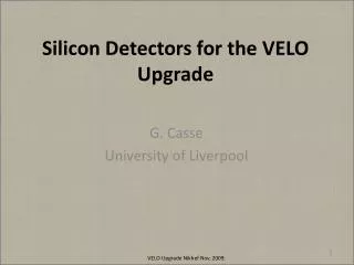
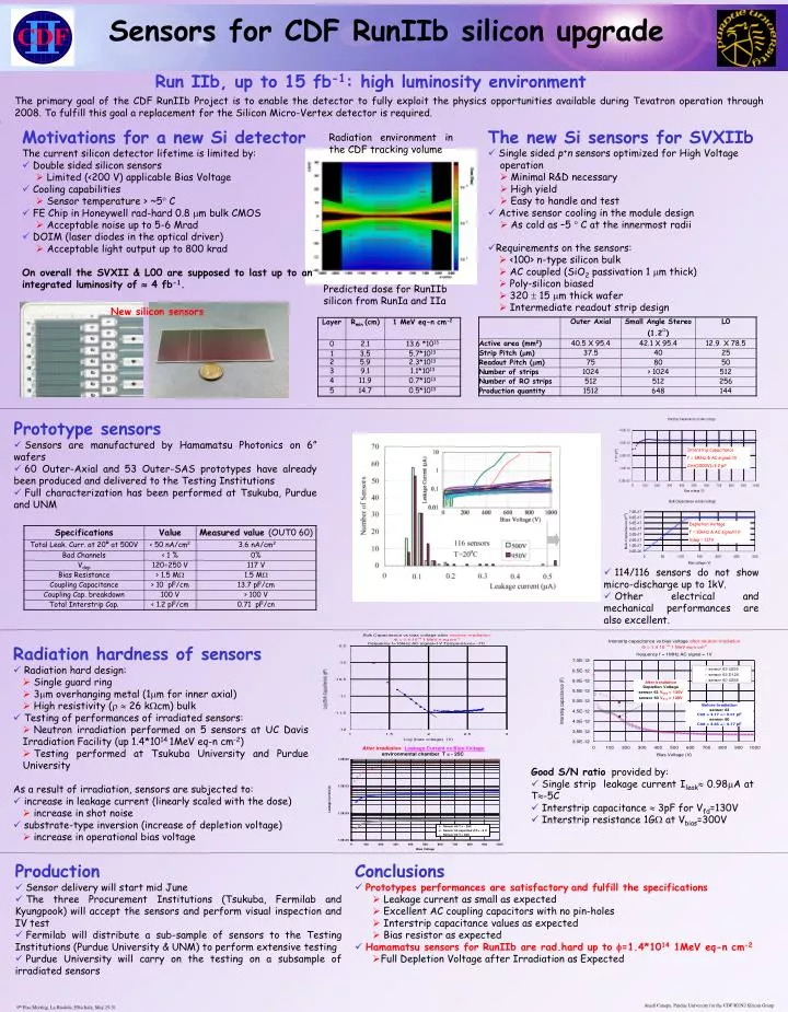
Motivations for a new Si detector The current silicon detector lifetime is limited by: Double sided silicon sensors Limited (<200 V) applicable Bias Voltage Cooling capabilities Sensor temperature > ~5 C FE Chip in Honeywell rad-hard 0.8 m m bulk CMOS

E N D
Motivations for a new Si detector The current silicon detector lifetime is limited by: • Double sided silicon sensors • Limited (<200 V) applicable Bias Voltage • Cooling capabilities • Sensor temperature > ~5 C • FE Chip in Honeywell rad-hard 0.8 mm bulk CMOS • Acceptable noise up to 5-6 Mrad • DOIM (laser diodes in the optical driver) • Acceptable light output up to 800 krad On overall the SVXII & L00 are supposed to last up to an integrated luminosity of 4 fb-1. • The new Si sensors for SVXIIb • Single sided p+n sensors optimized for High Voltage operation • Minimal R&D necessary • High yield • Easy to handle and test • Active sensor cooling in the module design • As cold as –5 C at the innermost radii Radiation environment in the CDF tracking volume • Requirements on the sensors: • <100> n-type silicon bulk • AC coupled (SiO2 passivation 1 mm thick) • Poly-silicon biased • 320 15 mm thick wafer • Intermediate readout strip design Predicted dose for RunIIb silicon from RunIa and IIa New silicon sensors Interstrip Capacitance f = 1MHz & AC signal=1V Cint(1000V)=3.2 pF Depletion Voltage f = 10kHz & AC signal=1V Vdep = 117V Sensors for CDF RunIIb silicon upgrade Run IIb, up to 15 fb-1: high luminosity environment The primary goal of the CDF RunIIb Project is to enable the detector to fully exploit the physics opportunities available during Tevatron operation through 2008. To fulfill this goal a replacement for the Silicon Micro-Vertex detector is required. • Prototype sensors • Sensors are manufactured by Hamamatsu Photonics on 6” wafers • 60 Outer-Axial and 53 Outer-SAS prototypes have already been produced and delivered to the Testing Institutions • Full characterization has been performed at Tsukuba, Purdue and UNM • 114/116 sensors do not show micro-discharge up to 1kV. • Other electrical and mechanical performances are also excellent. • Radiation hardness of sensors • Radiation hard design: • Single guard ring • 3mm overhanging metal (1mm for inner axial) • High resistivity (r 26 kWcm) bulk • Testing of performances of irradiated sensors: • Neutron irradiation performed on 5 sensors at UC Davis Irradiation Facility (up 1.4*1014 1MeV eq-n cm-2) • Testing performed at Tsukuba University and Purdue University • As a result of irradiation, sensors are subjected to: • increase in leakage current (linearly scaled with the dose) • increase in shot noise • substrate-type inversion (increase of depletion voltage) • increase in operational bias voltage Good S/N ratio provided by: • Single strip leakage current Ileak 0.98mA at T-5C • Interstrip capacitance 3pF for Vfd=130V • Interstrip resistance 1GW at Vbias=300V • Production • Sensor delivery will start mid June • The three Procurement Institutions (Tsukuba, Fermilab and Kyungpook) will accept the sensors and perform visual inspection and IV test • Fermilab will distribute a sub-sample of sensors to the Testing Institutions (Purdue University & UNM) to perform extensive testing • Purdue University will carry on the testing on a subsample of irradiated sensors • Conclusions • Prototypes performances are satisfactoryand fulfill the specifications • Leakage current as small as expected • Excellent AC coupling capacitors with no pin-holes • Interstrip capacitance values as expected • Bias resistor as expected • Hamamatsu sensors for RunIIb are rad.hard up to =1.4*1014 1MeV eq-n cm-2 • Full Depletion Voltage after Irradiation as Expected Anadi Canepa, Purdue University for the CDF RUN2 Silicon Group 9th Pisa Meeting, La Biodola, Elba Italy, May 25-31