Understanding Transistor Fabrication, Behavior, and Parasitics: A Comprehensive Guide
210 likes | 293 Views
This guide provides detailed insights into the basic steps of transistor fabrication, various transistor structures, behavior characteristics, and common parasitic elements. Learn about IC fabrication processes, transistor layouts, current characteristics, and solutions to latch-up issues. Discover the significance of transistor parasitics, such as gate capacitance, source/drain capacitance, and resistance. Understand latch-up in CMOS ICs, its causes, and effective solutions to prevent chip damage. Enhance your knowledge of transistor technology with this comprehensive resource.

Understanding Transistor Fabrication, Behavior, and Parasitics: A Comprehensive Guide
E N D
Presentation Transcript
Topics • Basic fabrication steps. • Transistor structures. • Basic transistor behavior. • Latch up.
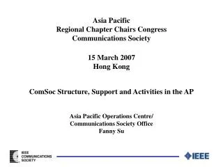
Fabrication processes • IC built on silicon substrate: • some structures diffused into substrate; • other structures built on top of substrate. • Substrate regions are doped with n-type and p-type impurities. (n+ = heavily doped) • Wires made of polycrystalline silicon (poly), multiple layers of aluminum/copper (metal). • Silicon dioxide (SiO2) is insulator.
transistor via Simple cross section SiO2 metal3 metal2 metal1 poly substrate n+ n+ p+ substrate
Photolithography Mask patterns are put on wafer using photo-sensitive material:
Process steps First place tubs to provide properly-doped substrate for n-type, p-type transistors: p-tub n-tub substrate
Process steps, cont’d. Pattern polysilicon before diffusion regions: gate oxide poly poly p-tub n-tub
Process steps, cont’d Add diffusions, performing self-masking: poly poly p-tub n+ n+ n-tub p+ p+
Process steps, cont’d Start adding metal layers: metal 1 metal 1 vias poly poly p-tub n+ n+ n-tub p+ p+
Level 2 metal • Polish SiO2 before adding metal 2: metal 2 metal 1 metal 1 vias poly poly p-tub n+ n+ p-tub p+ p+
Transistor structure n-type transistor:
Transistor layout n-type (tubs may vary): L w
Drain current • Linear region (Vds < Vgs - Vt): • Id = k’ (W/L)(Vgs - Vt)(Vds - 0.5Vds2) • Saturation region (Vds >= Vgs - Vt): • Id = 0.5k’ (W/L)(Vgs - Vt) 2
90 nm transconductances Typical parameters: • n-type: • kn’ = 13 A/V2 • Vtn = 0.14 V • p-type: • kp’ = 7 A/V2 • Vtp = -0.21 V
Current through a transistor Use 90 nm parameters. Let W/L = 3/2. Measure at boundary between linear and saturation regions. • Vgs = 0.25V: Id = 0.5k’(W/L)(Vgs-Vt)2= 0.12 A • Vgs = 1V: Id = 7.2 mA
Basic transistor parasitics • Gate to substrate, also gate to source/drain. • Source/drain capacitance, resistance.
Basic transistor parasitics, cont’d • Gate capacitance Cg. Determined by active area. • Source/drain overlap capacitances Cgs, Cgd. Determined by source/gate and drain/gate overlaps. Independent of transistor L. • Cgs = Col W • Gate/bulk overlap capacitance.
Latch-up • CMOS ICs have parastic silicon-controlled rectifiers (SCRs). • When powered up, SCRs can turn on, creating low-resistance path from power to ground. Current can destroy chip. • Early CMOS problem. Can be solved with proper circuit/layout structures.
Parasitic SCR circuit I-V behavior
Solution to latch-up Use tub ties to connect tub to power rail. Use enough to create low-voltage connection.