Understanding MPC555 Bus Protocols and Interfacing Basics
Learn about the basic bus protocol of MPC555, including asynchronous communication with REQ#, ACK#, Data, ADS, and CMD, for read and write transactions. Explore the timing, control lines, read and write processes, and complexities of the MPC555 bus.

Understanding MPC555 Bus Protocols and Interfacing Basics
E N D
Presentation Transcript
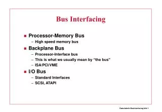
Bus basics • I/O transactions • MPC555 bus • Reference: • Chapter 9 of MPC555 User’s Manual Bus Protocols and Interfacing
Basic example • Discuss a basic bus protocol • Asynchronous (no clock) • Initiator and Target • REQ#, ACK#, Data[7:0], ADS[7:0], CMD • CMD=0 is read, CMD=1 is write. • REQ# low means initiator is requesting something. • ACK# low means target has done its job. REQ# = REQ
A read transaction • Say initiator wants to read location 0x24 • Initiator sets ADS=0x24, CMD=0. • Initiator then sets REQ# to low. (why do we need a delay? How much of a delay?) • Target sees read request. • Target drives data onto data bus. • Target then sets ACK# to low. • Initiator grabs the data from the data bus. • Initiator sets REQ# to high, stops driving ADS and CMD • Target stops driving data, sets ACK# to high terminating the transaction
0x24 ?? ?? ADS[7:0] CMD Data[7:0] REQ# ACK# 0x55 ?? ?? A B C D E F G HI Read transaction
A write transaction (write 0xF4 to location 0x31) • Initiator sets ADS=0x31, CMD=1, Data=0xF4 • Initiator then sets REQ# to low. • Target sees write request. • Target reads data from data bus. (Just has to store in a register, need not write all the way to memory!) • Target then sets ACK# to low. • Initiator sets REQ# to high & stops driving other lines. • Target sets ACK# to high terminating the transaction
ADS[0] ADS[1] Delay ACK# ADS[2] ADS[3] ADS[4] ADS[5] ADS[6] ADS[7] Data[0] REQ# .. .. .. .. .. 0 Data[7] Button (0 or 1) The push-button(if ADS=0x04 write 0 or 1 depending on button) What about CMD?
ADS[0] DATA[0] ADS[1] DATA[1] ADS[2] DATA[2] Delay ACK# ADS[3] DATA[3] D DATA[4] ADS[4] ADS[5] DATA[5] clock ADS[6] DATA[6] Flip-flop which controls LED ADS[7] DATA[7] REQ# The LED(1 bit reg written by LSB of address 0x05)
MPC555 Bus The basic function of the MPC555 bus is similar, though slightly more complicated. (Chapter 9 of 555 User’s Manual) • Timing is controlled by a global clock; all signals are in reference to the rising edge of this clock. • 32-bit data bus D[0:31] • 24-bit address bus A[8:31] • A[0:7] not sent off chip • On-chip peripherals still see 32 address bits • Basic control lines: • RD/#WR • #TS (transfer start)—like #REQ but only asserted on first • clock cycle of transaction • #TA (transfer acknowledge)—like #ACK
MPC555 Read • Master drives address, RD/#WR, and #TS to initiate a read transaction. Address and RD/#WR guaranteed valid at same rising clock edge that #TS is asserted. Master deasserts #TS after one cycle, but keeps driving address and RD/#WR until it sees #TA. • Slaves look at address and RD/#WR when #TS asserted. One of them will drive data and assert #TA. Master samples data on same rising clock edge when #TA is asserted. • Minimum transactions takes two clock cycles. • Transactions can take longer • slow slaves add wait states by not asserting #TA.
MPC555 Read(s) CLK A[8:31] ?? A1 ?? A2 ?? D[0:31] ?? D1 ?? D2 ?? RD/#WR ?? ?? ?? #TS #TA read @ A1 read @ A2
MPC555 Write • Same start as for a read, except for polarity of RD/WR#. • Master drives data by 2nd cycle. • Slaves look at address and RD/#WR when #TS is asserted. One of them will read data and assert #TA. • As with reads, minimum transaction length is two cycles. Slaves can take longer, however, by not asserting #TA. Master keeps driving address, RD/#WR, and data until it sees #TA asserted.
MPC555 Write CLK A[8:31] ?? A1 ?? A2 ?? D[0:31] ?? D1 ?? D2 ?? RD/#WR ?? ?? ?? #TS #TA write @ A1 write @ A2
Of course, things aren’t that simple • TSIZ[0:1] – Specifies the size of the data to be transferred. (aka “Port Size”) • #Burst – Indicates a burst transaction • #BDIP – Burst Data In Progress (more burst stuff) • #BI – Burst Inhibit. Indicates that the slave doesn’t support burst transactions • Many More…
Example of complexity:The Burst Mechanism (9.5.3) • Burst transfers are used to move (up to) 16 bytes at a time • #BURST must be asserted by master • #BI must not be asserted by slave • Must be a 16-byte aligned access • Supports critical word first.
Arbitration (9.5.6) Requesting device Arbiter • Request the bus • Assert #BR • Grant bus arbitration • Assert #BG • ACK bus mastership • Wait for #BB to be deasserted • Assert #BB • Negate #BR • Terminate Arbitration • Negate #BG Perform data transfer • Release bus mastership • Negate #BB
Transfer Alignment 0x1000 0 7 8 15 16 23 24 31 • MPC555 external bus supports natural address alignment • Byte access: Any address alignment • Half-word access: Address bit 31 equal to 0 • Word access: Address bits 31 and 30 equal to 0
Dealing with Smaller Accesses: Reads 0x1000 0 7 8 15 16 23 24 31 • Assume that the word value 0x12345678 is stored at 0x1000 and that r4 contains 0x1000. What happens on the following transfers? • D[0:7] D[8:15] D[16:23] D[24:31] • lbz r3 , 0 (r4) • lbz r3 , 1 (r4) • lbz r3 , 2 (r4) • lbz r3 , 3 (r4) • lhz r3 , 0 (r4) • lhz r3 , 2 (r4)
Dealing with Smaller Accesses: Writes 0x1000 0 7 8 15 16 23 24 31 • How about the following transfers? • D[0:7] D[8:15] D[16:23] D[24:31] • stb r2 , 0 (r4) • stb r2 , 1 (r4) • stb r2 , 2 (r4) • stb r2 , 3 (r4) • sth r2 , 0 (r4) • sth r2 , 1 (r4)
Dealing with Smaller Accesses • On a write access, which two factors determine which bits in a 32-bit word are updated? • On most wide buses, the master drives byte enable lines instead of less significant address bits • Moto 68000 (16 bits): #LDS, #UDS (no address LSB) • 32-bit buses: Replace low 2 address bits with 4 byte enables • MPC555 does not: • Full byte address provided • Size (byte, halfword, word) encoded on two control lines TSIZ[0-1]
Unaligned Accesses 0x1004 0x1000 0 7 8 15 16 23 24 31 • Consider two adjacent 32-bit memory locations and assume that r4 = 0x1000. What happens when the CPU executes the following instructions? • lwz r3 , 2 (r4) • lwz r3 , 1 (r4)
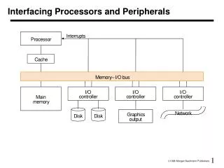
Basic bus issues • What are the basic wires for specifying the transaction and moving the data? • What are the types of transactions? How are they specified? • How is length of data transfer specified? • Who can delay (insert wait states?) • How is arbitration done? • Out-of-order transfers allowed? • Any restrictions? • Error reporting? • Weirdness? • Alignment for example.
Transaction types • Usually read/write with a length • But in a given domain, other info might be important. • Data vs. Code access. • I/O vs. memory access • Hints to target device • Length might be arbitrary.
Delaying • Who can delay and how • Usually a target (slave) can delay • Sometimes initiator (master) can delay • Sometimes initiator can drop the transaction • Sometimes the target has options on how to delay.
Arbitration • Fairness • Even sharing, priority sharing, weighted sharing • Mechanism • Centralized arbiter • Distributed arbiter • Combination • Duration • Until done • Until someone else requests • Until certain time passes. • Combination
Out-of-order • Does the bus allow transactions to complete out-of-order? • If so, can increase bandwidth (why?) • If so, might have to worry about ordering issues • Memory consistency models not a topic for this class (take CE 452!) but basics are pretty easy to grasp
Processor 1 Write I=1 Write J=1 Processor 2 Write J=2 Write I=2 Out-of-order: Ordering problem If both programs are executed in order, is there any setting of J and I which is impossible?

