Download
1 / 32
320 likes | 526 Views
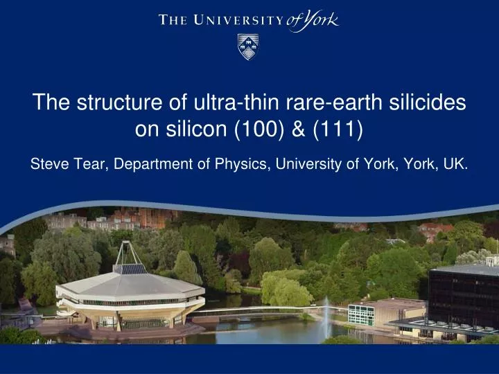
The structure of ultra-thin rare-earth silicides on silicon (100) & (111). Steve Tear, Department of Physics, University of York, York, UK. Introduction.

E N D
The structure of ultra-thin rare-earth silicides on silicon (100) & (111) Steve Tear, Department of Physics, University of York, York, UK.
Introduction • Interests are in surface and interface structure and, more recently, the correlation of the structure with electronic, magnetic and transport properties. • Detailed knowledge of the structure of surfaces, interfaces and nanostructures is a key component in the quantitative understanding of their chemical, electronic and magnetic properties. • Interfaces are one of the central features of spintronic devices and quality is important to their ultimate performance. • One of the key interfaces for hybrid spintronic devices is the ferromagnetic-semiconductor interface for spin injection.
Introduction Rare earth silicides on silicon (100) & (111) Results of structure analyses of ultra-thin films of silicides Cooling during growth process may have beneficial effect for outcome of final structure: Mn on 2D RE silicide and Si on 2D RE silicide.
Techniques • Experimental equipment at York (UHV):- • Low-energy electron diffraction (LEED) • Omicron scanning tunnelling microscope (STM) • STFC Daresbury:- • Medium-energy ion scattering (MEIS). • York JEOL Nanocentre:- • JEOL 2200FS double aberration-corrected scanning transmission electron microscope (AC-STEM)
Rare earth silicides Rare earth (lanthanides) metals • Divalent or trivalent: 4fn(5d6s)2 or 4fn(5d6s)3 • Gd, Tb, Dy, Ho, Er, Tm, trivalent; Y • Sm trivalent /divalent. • Eu, Yb, Nd, divalent. • Majority of trivalent rare earths have hcp structure. Rare earth silicides • Disilicides (RESi2–X , x~0.3): hexagonal, tetragonal, or ortho. • On Si(111): hex. RE silicides(0001) lattice match (~few %)* • On Si(100): silicide nanowires are formed 10 nm x ~1 m, hexagonal, tetragonal, or orthorhombic? * J Knapp and S Picraux. Appl. Phys. Lett. 48, 466(1986)
MEIS: principles of structure analysis 100keV H+ Ho • Double alignment:- • Shadowing — align incident ion beam to gain surface sensitivity Si Counts Scattered ion energy • Blocking — detect angle-dependent scattered ion yield; • Dips in yield correspond to positions of surface atoms Scattering angle
<100> Yield 4 5 5 0 5 5 6 0 6 5 S c a t t e r i n g a n g l e / d e g r e e s MEIS: Si(111)(1x1)-RE 100keV H+ 2D silicides: Si(111)(1x1)-RE (RE = Y, Gd, Dy, Ho, Er, Tm) Ho 1 ML of Ho deposited onto Si(111) held at 550°C for 10 mins. Si Scattered ion energy Counts Scattering angle Wood T et al. Phys. Rev. B 72, 165407 (2005).
Si(111)1×1-Gd Si(111)1×1-Y Si(111)1×1-Er Si(111)1×1-Dy Si(111)1×1-Tm Si(111)1×1-Ho MEIS: Si(111)(1x1)-RE Wood T et al. Phys. Rev. B 72, 165407 (2005).
MEIS: Si(111)(1x1)-RE Bulk RE-Si2 bond length:- 3.060 Å (Gd) – 2.979 Å (Tm) Structural parameters obtained from MEIS for the 2D RE silicides on Si(111). Errors have been obtained via the 2R-factor. Wood T et al. Phys. Rev. B 72, 165407 (2005).
Strain in the 2D silicides • Compare effective c-axis strain with the a-axis strain in a bulk RE silicide distorted to fit Si(111). • Plotted as a function of lattice mismatch • The a-axis strain which results from the lattice mismatch is compensated for by strain in the c-axis which acts to maintain constant density in the surface silicide layer Tm Er Ho DyY Gd
Growth on 2D RE silicide Motivation 2D layer offers passivated silicon terminated (1x1) surface, stable up to ~600°C. Template for further growth on a ideal silicon surface. Bury delta-layer of rare earth in silicon? Modification of metal-semiconductor interface – spintronics? Experimental Create 2D silicide: 1 ML of Ho onto Si(111) held at 550°C Cool to ~ minus 100°C. 1. Si:- Deposit 6 ML of silicon. Post anneal at 400°C for 10 mins. 2. Mn:- Deposit 3 ML of manganese. Post anneal at 300°C for 1 min.
Si/Ho/Si(111) A-type orientation of silicon overlayers on 2D Re-silicide.
Silicon / Ho / Si(111) <110> <100> Experimental MEIS data compared with simulations for a double bilayer of a-type Si above a 2D Ho layer.
Si / Ho / Si(111) Include 7x7 surface termination of added silicon layers in simulation <110> <100> Experimental MEIS data compared with simulations for a double bilayer of a-type Si above a 2D Ho layer and added silicon surface terminated by 7x7.
STM: Mn on 2D RE silicide 50 nm x 50 nm 2 ML Mn on RT silicide 2ML Mn on cooled 2D RE silicide + 1 min anneal at 250C 4 ML Mn on cooled 2D RE silicide + 1 min 250°C anneal 300 nm x 300 nm 20 nm x 20 nm M Reakes et al J Phys Cond. Matter, 21 265001 (2009)
MEIS: energy spectra Experimental spectra compared to simulations (smooth line): Mn layer above 2D HoSi on Si Mn layer below Si and above Ho Mn layer above Ho on Si
STM: RE silicide nanowires on Si(100) Sub-ML coverages of Ho deposited onto clean Si(001) substrates at between 500 – 600°C with no post anneal c(2x2) 0.25 ML Ho , 700 x 700 nm2 0.3 ML Ho , 100 x 100 nm2 The NWs have widths in the range 1.5 – 5 nm and lengths ~300 nm or more Strong reordering of step edges as Si atoms are donated to forming silicide Tetragonal or Hexagonal NW silicide? D. R. Bowler, J. Phys.: Cond. Matter 16, R721 (2004) Chen et al., Appl. Phys. Lett. 76, 4004 (2000)
MEIS data6ML Holmium on Si(100) at -180°C/650°C vs 650°C <110> geometry <110> geometry Cooled growth + 650°C anneal 650°C growth exptvshexagonalsimulation 650°C growth exptvstetragonal simulation (c-axis = 13.12 Å).
Summary • MEIS has enabled precise determination of strain in 2D RE silicides • Using MEIS has identified the hexagonal silicide grown on cooled Si(100) but tetragonal silicide when grown @ 650°C – implications for electronic properties of interface. • MEIS has provided some detailed information on 2D RE silicide as template for Mn and Si overlayer growth on cooled surface –buried delta-RE layer and modification of interface structure
Future work • MEIS: structure of initial interface formation: dependence • on initial surface structure, for example. • non-destructive c.f. AC-STEM • Structure of nanowires on surfaces • Full 2D energy loss & scattering angle analysis • SBH of metal – silicon vs metal – 2D RE silicide – silicide • Calculation of interface structures using CASTEP • Calculation of SBH using modified CASTEP
Acknowledgements Dr Matt Probert (CASTEP) Dr Phil Hasnip Dr Paul Bailey (Daresbury) Dr Tim Noakes (Daresbury) Tim Wood Ed Perkins Mike Reakes Charles Woffinden Andrew Vick Jeremy Mitchell Dr Chris Eames Dr Chris Bonet York-JEOL Nanocentre
HAADF AC-STEM: Er silicide NW on Si(100) Hex [01-10] [0001] [001] 1nm [1-10]
AC-STEM: Er silicide NW on Si(100) 1nm Tet [001] [100] [001] [1-10]
Interfaces Overview Hexagonal Tetragonal Hexagonal nanowires have stepped interfaces Tetragonal nanowirestend to have regular defects along the interface
I/V between two islands Initial fit for curve Schottky barrier height=0.48eV
Conduction along Nanowire • Resistance of 54.5 kΩ
SB: NW to silicon substrate Initial fit for curve Schottky barrier height=0.53eV NW sample transferred in vac suitcase to reduce oxidation
Vacuum Schottky Barrier ht C.B. Fermi level V.B. Metal n-type semiconductor Schottky Barrier Electrical properties of junction: Ohmic or Schottky barrier I 0 V metal +ve w.r.t. semiconductor