Download
1 / 63
760 likes | 1.08k Views
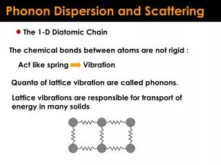
Act like spring Vibration. Phonon Dispersion and Scattering. The 1-D Diatomic Chain. The chemical bonds between atoms are not rigid :. Quanta of lattice vibration are called phonons. Lattice vibrations are responsible for transport of energy in many solids. Spring-mass model.

E N D
Act like spring Vibration Phonon Dispersion and Scattering • The 1-D Diatomic Chain The chemical bonds between atoms are not rigid : Quanta of lattice vibration are called phonons. Lattice vibrations are responsible for transport of energy in many solids
Spring-mass model harmonic oscillator Equation of motion : Solution : Natural frequency :
Lattice vibrations with monatomic basis Assumption All the atoms and the springs between them are the same The force on the n-th atom is only by its neighboring atoms Equilibrium Position : Deformed position :
Solution Substitute into equation
Frequency, w 0 Wavevector, k First Brillouin zone : Dispersion relation Slope( ) = Group velocity 1st Brillouin zone :
Group velocity transmission velocity of a wave packet - Beats - Wave packet or Wave group The velocity of energy propagation in the medium This is zero at the edge of the zone Standing wave
- : Long wavelength or continuum limit Frequency, w 1 - : Edge of first Brillouin zone Edge of First Brillouin zone 0 Wavevector, k • Acoustic branch : Velocity of sound in a crystal Acoustic branch Speed of sound Standing wave
Lattice vibrations with Two atoms per primitive basis • two atoms per unit cell
Solution Substitute into equation The determinant must be zero for nontrivial solutions
Two roots for Optical branch Acoustic branch
Optical branch and Acoustic branch Acoustic branch : The atoms move together, as in long wavelength acoustical vibration. Optical branch : If the two atoms carry opposite charges, we may excite a motion of this type with the electric field of a light wave. Influences optical properties of a crystal Optical branch
Between and • :no solution First Brillouin zone • Characteristics of optical branch : Group velocity is negligible High frequency
us-1 us us+1 us+2 us-1 us+1 us+2 us us+3 s-1 s s+1 s+2 s+3 • Transverse vs. Longitudinal polarization Three modes of wave vectors for one atom per unit cell Two transverse modes One longitudinal mode
Dispersion Relation for Real Crystal - Number of branches If there are q atoms in the primitive cell, there are 3q branches to the dispersion relation 3 acoustic branches : 1 longitudinal acoustic (LA) 2 transverse acoustic (TA) 3q - 3 optical branches : q - 1 longitudinal optical (LO) 2q - 2 transverse optical (TO)
- SiC - Si[100] direction Frequency gap The group velocity of phonons in the optical branches is small contribute little to the thermal conduction At low temperatures : TA are dominant contributors to the heat conduction At high temperatures : LA are dominant contributors to the heat conduction
Phonon scattering • Phonon-phonon scattering Governs the thermal transport properties of dielectric and semiconductor Inelastic scattering : the phonon frequency before the scattering event is different from that after the event Normal (or N) – process : Inside the 1st brillouin zone : energy conservation : crystal momentum conservation
Umklapp(or U) process : Outside the 1st brillouin zone N process U process
N-process vs. U-process U - process N - process Energy Conservation Conserved Conserved Net momentum not conserved Momentum Conservation Conserved Thermal conductivity Dominant Not dominant Act as a direct resistance to heat flow Distributing the phonon energy Thermophysical role
Scattering rate of the U-process Positive constants - Fig. 5.13 Thermal conductivity of silicon Phonon scattering: Temperature dependence Above room temperature Below room temperature At high temperature specific heat does not change significantly
1 3 1 2 2 3 1 2 4 3 4 4 • Phonon scattering – 4 phonon & defect Four – phonon scattering (Temperature range : 300 K ~ 1000 K) : Negligible Phonon – defect scattering Elastic scattering Independent of temperature Defendant on the phonon wavelength
Phonon scattering- phonon-electron Dominant at high temperature Scattering by acoustic phonon is essentially elastic. negligible Scattering by optical phonon is inelastic : Polar scattering Facilitates heat transfer between optical phonon and electron (Joule heating) : energy conservation : momentum conservation + : phonon absorption - : phonon emission (i : initial state f : final state)
Phonon scattering- Raman scattering Phonon and photon inelastic scattering called Raman scattering, X-ray scattering, neutronscattering, and Brillouin scattering Stokes shift (phonon emission) anti-Stokes shift (phonon absorption) i: incident photon s: scattered photon ph: phonon
Dependence on temperature used for surface temperature measurements
Electron Emission and Tunneling • Photoelectric Effect: Photoemission electromagnetic wave metal plate Heinrich Hertz observed the photoemission in 1887 J. J. Thomson discovered electron as a subatomic particle Albert Einstein explained the photoelectric effect in 1905 (Nobel Prize in 1921)
Measuring the Ejected Photoelectrons incident photon electrode electrode vacuum load A threshold frequency for photoemission in given material Frequency, n of incident radiation is not high enough no electric current
maximum kinetic energy of ejected electron • Work Function y electron right at the Fermi level work function: energy needed to remove electron from metal Ag, Al, Au, Cu, Fe: 4 ~ 5 eV (ultraviolet region) Na, K, Cs, Ca: 2 ~ 3 eV (visible region) A photon can interact only one electron at a time.
Application of Photoemission XPS (x-ray photoelectron spectroscopy) measurement of the electron binding energy, Ebd chemical composition of the substance near the surface sample electron energy analyzer
current density • Thermionic Emission Similarity to photoemission → Work function cold hot vacuum Load J A
EF Fermi-Dirac distribution at T = 0, E < EF, all states are filled by electron and E > EF all states are empty • when T > 0, • Some electron having more than EF + y, • Small fraction of electron must occupy energy levels exceeding EF + y.
velocity space: : fraction of electron reflected • Current Density Particle flux Current density
Recall number of electrons per unit volume current density in the x direction ejected velocity (vx) of electron > binding Ebd
when less than 2% error
Richardson-Dushman eq. Richardson constantARD = 1.202×10⁶ A/(m2K2)
: average energy of the “hot electron” • Heat Flux heat transfer associated with electron flow Flux of energy → similarity to current density
Let • Derivation of Heat Flux
Field Emission and Electron Tunneling Thermionic emission may be enhanced or even reversed by an applied electric field Potential U • Field emission When the field strength is very high, electrons at lower energy levels than the height of the barrier can tunnel through the potential hill. Electron wave Tunnel Electron energy • Current density Potential barrier (hill), y Fowler-Nordheim equation d(x) : width of potential at E
Time dependent Schrödinger equation • Current Density Electron motion: governed by Schrödinger’s wave equation Wavefunction form when E > U when E < U
kinetic energy in the x direction, E energy at the top of potential barrier, Emax reference energy, Emin number of available electrons, n(E) • Transmission probability or transmission coefficient • Tunneling current density
electric field, • Fowler-Nordheim tunneling Potential U Tunnel current density by various approximations chemical potential Energy barrier with two electrodes
Current density positive constant, C positive constant, a
Electrical Transport in Semiconductor Devices • Number Density, Mobility, and the Hall Effect • Number Density Number density of electrons and holes determines the electrical, optical, thermal properties of semiconductor materials. electron and hole → Fermi-Dirac distribution function number density of electrons and holes • EC: minimum of conduction band • EV: maximum of valence band
densities of states in the conduction and valance bands MC: number of equivalent minima in conduction band effective mass for density of states geometric average of 3 masses = longitudinal mass + 2 transverse mass
MC: number of equivalent minima in the conduction band • Most semiconductor can be described one band minimum at k = 0 as well as several equivalent anisotropic band minima k ≠ 0 • The energy is chosen to be to zero at the edge of the valence band. • Lowest band minimum at k = 0 is not the lowest minimum above the valence band • at • ( In here x = 5 nm-1) • There are 6 equivalent minima, these are minimum energy. On the other hand, maxima of valence band only has one k state. • So in calculation De, we must multiply 6 (MC) Simplified E-k diagram of silicon within the 1st Brillouin zone along the (100) direction
we have to consider the effective mass • The effective mass of electrons is a geometric average over the 3 major axes because the effective mass of silicon depends on the crystal direction. • The effective mass of holes is an average of heavy holes and light holes because there exist different sub-bands. • The effective mass calculation for density of states • = The geometric average of the 3 masses: • (one longitudinal mass ml, two transverse mass mt) • must include the fact that several equivalent minima exist : MC in the conduction band
At moderate temperatures, approximation with M-B distribution NC, NV: effective density of states in conduction band and valance band
number density for intrinsic and doped semiconductors thermally excited electron-hole pairs per unit volume number density of intrinsic carriers Fermi energy for an intrinsic semiconductor when ne = nh Fermi energy for an intrinsic semiconductor in the middle of the forbidden band or the bandgap
n-type impurities of donors (P, As) involved → ionization of donors increases the number of free electrons • p-type Impurities of acceptors (B, Ga) involved → Ionization of acceptors increases the number of holes • Fully ionized impurities, charge neutrality requirement NA, ND: number densities of donors and acceptors