Download
1 / 10
100 likes | 204 Views
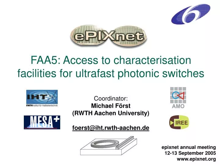
FAA5: Access to characterisation facilities for ultrafast photonic switches. Coordinator: Michael Först (RWTH Aachen University) foerst@iht.rwth-aachen.de. r = 20 µm. Research Integration Targets. FAA 5 Objectives:

E N D
FAA5: Access to characterisation facilities for ultrafast photonic switches Coordinator:Michael Först(RWTH Aachen University)foerst@iht.rwth-aachen.de
r = 20 µm Research Integration Targets • FAA 5 Objectives: • Combine the advanced facility for sub-picosecond characterisation of optical switching phenomena with know-how in the field of fabrication and modelling • Focus on switching devices based ondielectric (SOI, SiON) microring resonators • Enable comparison of different switchingconcepts / materials • Integration Targets: • Provide the facility for measurements of devices fabricated by partners • Take advantage of device simulations by partners for device design and for analysis of nonlinear optical characterization • Produce joint publications • Exploit Junior Researcher Exchanges
Progress measured against targets (1) • Provide the facility to activity partners • Two measurement batches in 1st year of ePIXnet (one set of measurements per year announced) • Characterisation of devices from at least two partners(samples from UT-MESA and AMO, as promised) • Delivery of first device device to characterisation facility (Milestone 11.2 at M12) • Prepare documentation • Description of the laboratory equipment and available measurement techniques published on ePIXnet webpage • Junior Researcher Exchanges • 4 JRE’s within first year(in average one per partner per year, as promised)
Progress measured against targets (2) • Device simulation • First results of device simulations provided to fabrication facilities to assist device design (Milestone 11.1 at M6) • Response of a resonator device with fast Kerr-type ((3)) nonlinearity in the microring to optical pulses • Additional simulation tool developed to solve nonlinear Schrödinger Equation for analysis of nonlinear propagationeffect in straight waveguides • Prepare joint publications • “Time-resolved analysis of all-optical switching in SOI ring resonators”, to be submitted, joint by 2 partners(one joint publication per year announced) Simulations by IREE ()
Research highlights (1) Device fabricated by UT-MESA • Nonlinear effects in straight SOI waveguides • Spectral transmissioncharacteristics of 200 fspulses at 1.55 µm • Spectral broadening of input pulse due to non-linear (3)effects • Indication of Raman gain at 1650 nm • Preliminary simulation resultsby solving modified NLSE based on split step Fouriermethod
Research highlights (2) Device fabricated by AMO • Time-resolved analysis of all-optical switching in SOI microring resonators at 1.53 µm • Spectrally and time-resolved analysis of the drop port signalupon optical carrier injection(vert. geometry, linear absorption) • Resonance shift due to thermal loading (accumulation, red) and plasma dispersion effect (green) • Picosecond all-optical switching demonstrated as intensity modulations at resonances for positive and negative time delays • See FAA 5 poster presentation for details ∆t < 0 ∆t > 0
Additional work • So far, no work planned/realised with additional consumable budgets • Junior Researcher Exchange of FAA5 partner UT-MESA (D. Geuzebroek) to Heinrich-Hertz Institut, Berlin (JRA6 member) • Successful demonstration of 40 GBit/s transmission through a Reconfigurable Optical Add Drop Multiplexer (ROADM) consisting of Si3N4 microring resonators
Junior Exchanges • Douwe Geuzebroek(UT-MESA HHI) 11–15 April 2005 • 40GBit/s transmission through a Reconfigurable OpticalAdd Drop Multiplexer consisting of Si3N4 microring resonators(at Heinrich Hertz Institute,Berlin) • Ronald Dekker(UT-MESA RWTH Aachen) 2–3 June 2005 • Nonlinear analysis of SiON waveguides Observation of soliton formation • Ronald Dekker(UT-MESA RWTH Aachen) 22–26 August 2005Frantisek Ondracek(IREE RWTH) 22–26 August 2005 • Observation of Raman gain in Si waveguides • Linear and nonlinear analysis of Si3N4 microring resonators • Jan Niehusmann(RWTH IREE) planned for October 2005 • Detailed analysis of experimental switching results by comparisonto simulation studies
Problems & actions • The number of partners using this facility is rather small (as pointed out at the Feb. 2005 AC meeting) • to tackle this “problem”, a description of the facilityequipment and measurement techniques is presentedon the ePIXnet website • other consortium partners are invited to carry out sub-picosecond time-resolved experiments at the facility
M12-30 Planning • Detailed planning for M12-24 • Continue switching analysis of SOI microring resonatorswith additional nonlinear materials (e.g., carbon nanotubes) • Start analysis of all-optical switching in Si3N4 resonators(so far only linear characterisation) • Extent simulation models taking into account plasma-dispersion effect due to optical carrier injection • Del. 11.2 (M18): Full characterisation of all-optical switching in either SOI or SiON devices • Targets for M25-30 • Extent the optical switching analysis to low-cost polymer microring resonators • Fabricate ion-damaged SOI resonators with reduced carrier lifetimes to increase all-optical switching speed (for the caseof plasma-dispersion effect induced switching)