Download
1 / 7
70 likes | 217 Views
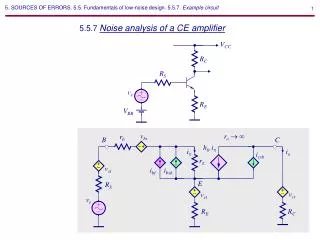
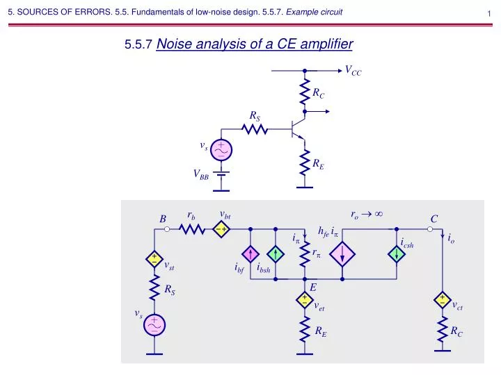
v bt. r b. B. C. h fe i p. i p. i o. i csh. r p. r o. v st. i bf. i bsh. E. R S. v ct. v et. v s. R E. R C. 5. SOURCES OF ERRORS. 5.5. Fundamentals of low-noise design . 5.5.7. Example circuit. 5.5.7 Noise analysis of a CE amplifier. V CC. R C. R S. v s. R E.

E N D
vbt rb B C hfe ip ip io icsh rp ro vst ibf ibsh E RS vct vet vs RE RC 5. SOURCES OF ERRORS. 5.5. Fundamentals of low-noise design. 5.5.7. Example circuit 5.5.7 Noise analysis of a CE amplifier VCC RC RS vs RE VBB ro
? vn s 5. SOURCES OF ERRORS. 5.5. Fundamentals of low-noise design. 5.5.7. Example circuit • Our final aim is to find and minimize the total input noise vn s. vbt rb B C hfe ip ip io icsh rp vst ibf ibsh E RS vet vct vs RE RC • Let us first find vn s by applying superposition.
io vs AOL 1+AOLb As =Gs + Gs bs fwd ___ _______ -hfe 1+hfe RE/(RE +RS+rb+rp) 1 RS+rb+rp+RE As= +0 ____________________ ___________ 5. SOURCES OF ERRORS. 5.5. Fundamentals of low-noise design. 5.5.7. Example circuit • 1) Signal gain As for vs, vst, vbt, and vet. vbt rb B C hfe ip ip io rp vst E RS vet vs RE RC
io ibf AOL 1+AOLb Abf =Gbf + Gbf bbf fwd ___ _______ RS+rb+RE RS+rb+RE +rp hfe 1+hfe RE/(RE +RS+rb+rp) Abf= +0 ____________________ ___________ 5. SOURCES OF ERRORS. 5.5. Fundamentals of low-noise design. 5.5.7. Example circuit • 2) Noise gain Abf for ibf and ibsh. rb B C hfe ip ip io rp ibf ibsh E RS vs RE RC
io icsh AOL 1+AOLb Acsh =Gcsh + Gcsh bcsh fwd ___ _______ hfe 1+hfe RE/(RE +RS+rb+rp) RE RE +RS+rb+rp Acsh= -1 ____________________ - ___________ 5. SOURCES OF ERRORS. 5.5. Fundamentals of low-noise design. 5.5.7. Example circuit • 3) Noise gain Acsh for icsh. rb B C hfe ip ip io icsh rp E RS vs RE RC
io vct Act =Dct ___ 1 RC Act= - ___ 5. SOURCES OF ERRORS. 5.5. Fundamentals of low-noise design. 5.5.7. Example circuit • 4) Noise gain Act for vct. rb B C hfe ip ip rp E RS io vs vct /RC RE RC
vn s (ibf +ibsh)Abf As icsh Acsh As vct Act As vn s(t) = vst +vbt +vet + + + __________ _______ _____ (RSbE+rp)2 hfe2 1 RC As2 +icsh2 + 4kT ________ _____ vn s2(f) = 4kTRSbE+(ibf 2+ibsh2)RSbE2 0 5. SOURCES OF ERRORS. 5.5. Fundamentals of low-noise design. 5.5.7. Example circuit • 5) Total input noise vs. time, vn s. rb B C hfe ip ip io icsh rp RS ibf ibsh E vs RE RC RSbE =RS +rb+RE