Download
1 / 15
150 likes | 168 Views
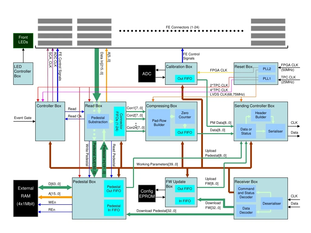
This system controls the signals and processes data for Front-End cards including connectors, LEDs, ADC, and more.

E N D
FE Connectors (1-24) Front LEDs SCA_CLK ADC CLK FE Control Signals Data In[215..0] A[5..0] FE Control Signals LED Controller Box Calibration Box Reset Box FPGA CLK (50MHz) ADC PLL2 FPGA CLK Out FIFO PLL1 TPC CLK (25MHz) 2*TPC CLK 4*TPC CLK LVDS CLK(68,75MHz) Read Box Controller Box Compressing Box Sending Controller Box Con1[7..0] Read Connector FIFOs (1-24) Pad-Row Builder Zero Counter Header Builder Con2[7..0] Read Ok Pedestal Substraction Event Gate PM Data[8..0] CLK Con24[7..0] Data or Status Serialiser Data[8..0] Out FIFO Data Pedestal Out[192..0] Write Pedestal Read Pedestal Pedestal In[191..0] Upload Pedestal[8..0] Working Parameters[39..0] Upload FW[8..0] Pedestal Box FW Update Box Receiver Box External RAM (4x1Mbit) D[63..0] Pedestal Out FIFO Config EPROM Out FIFO Command and Status Decoder A[15..0] CLK In FIFO Deserialiser WEn Pedestal In FIFO Data Download FW[32..0] Data Decoder REn Download Pedestal[32..0]
Reset Box • Prepare clocks for modules • TPC_CLKx2 (50 MHz) for Controller Box, Read Box and Pedestal Box • TPC_CLKx4 (100 MHz) for Controller Box • TPC_CLKx10 (250 MHz) for Controller Box • LVDS_CLK (68,75 MHz) for Sending Controller Box and Compressing Box • ASMI_CLK (20 MHz) for Firmware Update Box • MB_CLK (50 MHz) for Controller Box, Calibration Box and LED Controller Box • Prepare delayed reset for modules
Reset Box Clock Box FPGA_CLK (50 MHz) TPC_CLK (25 MHz) FPGA_Power_Good Soft_Reset TPC_CLKx2 TPC_CLKx4 TPC_CLKx10 MB_CLK LVDS_CLK ASMI_CLK Reset Signals PLL1 PLL2 ResetCounter
Controller Box • Prepare clock signals for Front-End cards • SCA CLK for shift register write and read (5 MHz or 10 MHz) • ADC CLK for ADC read-out (12,5 MHz) • Prepare control signals for Front-End cards • Shift register control signals • Amplifier control signals • ADC control signals • Prepare the Busy signal • Prepare the Trigger Counter • Read and evaluate the Working Parameter register
Controller Box Reset TPC_CLKx4 (100 MHz) TPC_CLKx10 (250 MHz) FPGA_CLK (50 MHz) TPC_CLKx2 (50 MHz) Timer Box SCA CLK Write Controller SCA_CLK ADC_CLK ADC CLK PreAmp_En WriteRead Reset_ShiftReg Analog_Reset ADC_Reset ADC_Load_Buffer Read Data FE_Command_Read Read_OK Event_OK FE_Command_Read_Req Trigger End_Of_Data_Block Working_Parameters Trigger LED Trigger_Counter[31..0] Trigger_LED MB_Busy Trigger Counter Busy
Read Box • Prepare Address signals for Front-End cards • ADC_OE for select the Front-End cards • A[5..0] for addressing the ADCs • Read the Front-End data • Read Pedestal for correction of Front-End data • Make Pedestal and threshold subtraction • Store the corrected Front-End data in the Connector FIFOs • Read the Front-End data • Write the Front-End data to the External Memory • Read and evaluate the Working Parameter register
Read Box Reset TPC_CLKx2 (50 MHz) Read_Data Read_Ok_Ack Pedestal_Memory_Ready Addressing A[5..0] ADC_OE Read_OK Event_OK Pedestal_Request Read_Pedestal Read FIFO Con_FIFO_Data[7..0] Con_FIFO_Read Con_FIFO_Data[7..0] Con_FIFO_Read D_In[215..0] FIFO Data_Strobe Write_Pedestal Pedestal_Mem_In[191..0] Pedestal_Mem_Out[191..0] Jumper_Settings Working_Parameters
Front-End read out sequences Write: 20,5us Read: 11,7ms Time Trigger Read 1. time slice Read 3. time slice Read 2. time slice Read 256. time slice Analog Reset: 5,6us Set Amplifiers: 10us Analog to Digital Conversion: 20us Data Read-out (2x32 ch.): 10,2us Read Data from FE2 Channel 32 Read Data from FE1 Channel 1 Read Data from FE1 Channel 2 Read Data from FE1 Channel 32
Front-End read-out timing Write: 41us (512*80ns) Read: 23,5ms ((5,6us+10us+20us+10,2us)*512) Analog Reset10us Set Ampl.10us Analog to Digital Conv.20us (256 ADC cycles) Read Card 1-22*5,1us Analog Reset5,6us Set Ampl.10us Analog to Digital Conv.20us (256 ADC cycles) PA_Enable/Reset Write/Read Reset_Shift_Reg Analog_Reset SCA_CLK (512 cycles) ADC_Reset ADC_Load_Buffer ADC_OE1 ADC_OE2 Connector 1 1.Data Out 2.Data Out 1.Data Out 2.Data Out Connector 2 Connector 24 1.Data Out 2.Data Out ADC_CLK
Compressing Box • Read the Connector FIFOs • Build data in Ped-row order • Make the zero compression • Add Mini Header to top of the data. • Store the compressed data in the Out FIFO • Store the compressed data in the External Memory, if Out FIFO full • Read and evaluate the Working Parameter register
Compressing Box Reset LVDS CLK (68,75 MHz) Read_OK Controller Read_OK_Ack Out_FIFO_Data[8..0] Out_FIFO_Read FIFO Zero Compressor Con_FIFO_Data[7..0] Con_FIFO_Read Event_OK Event_Processed_Ack Event_Processed External Memory Writer SRAM_FIFO_Write SRAM_FIFO_Data[64..0] FE_Command_Read Trigger_Counter Jumper_Settings Working_Parameters FE_Command_Read_Req
Read-out order of SR sector FIFO Con1A FIFO Con1B FIFO Con2A FIFO Con2B FIFO Con12A FIFO Con12B Multiplexer
Read-out order of HR sector FIFO Con1A FIFO Con1B FIFO Con2A FIFO Con2B FIFO Con12A FIFO Con12B Multiplexer
Ch N. Channel Chooser Box Write Controller Box Command Send Data Reader Status Req. Send Transmitter Box Busy Signal CLK Serialiser Data[7..0] Data Read and Send Data Status Ansver[31..0] XOFF SIU Interface Receiver Box Read Controller Box SIU Out FIFO Command and Status Decoder DataN[31..0] Packet and Header Builder CLK Deserialiser Data In FIFO Data Decoder Data[31..0] SIU Data[31..0] 32x SIU Controls Read Out Controller Ch 1. Write Controller Box Command Send SIU In FIFO Status Req. Send Transmitter Box Command Register CLK Serialiser Data[7..0] Data Read and Send Data Status Reader Status Ansver[31..0] XOFF Status Register Receiver Box Read Controller Box Command and Status Decoder Data1[31..0] Packet and Header Builder CLK Deserialiser Clock Box Data In FIFO 50MHz Data Decoder Data[31..0]