FERROELECTRIC RAM
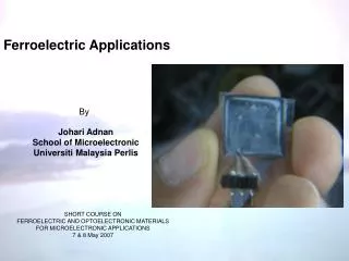
FERROELECTRIC RAM. OBJECTIVE OF THE PAPER Ferroelectric RAM (FeRAM or FRAM) is a random access memory similar in construction to DRAM but uses a ferroelectric layer instead of a dielectric layer to achieve non-volatility.

FERROELECTRIC RAM
E N D
Presentation Transcript
OBJECTIVE OF THE PAPER Ferroelectric RAM (FeRAM or FRAM) is a random access memory similar in construction to DRAM but uses a ferroelectric layer instead of a dielectric layer to achieve non-volatility. FeRAM is one of a growing number of alternative non-volatile memory technologies that offer the same functionality as Flash memory. INTRODUCTION
FeRAM is competitive in niche applications where its operating characteristics give it an advantage over Flash. The advanced smart card is a promising technology to extend information-providing services from terminal (PC and mobile phone) FeRAM can improve the transaction time in transportation applications through its fast programming time. SCOPE OF THE TOPIC
Development of FeRAM began in the late 1980s. Work was done in 1991 at NASA's Jet Propulsion Laboratory on improving methods of read out, including a novel method of non-destructive readout using pulses of UV radiation. Much of the current FeRAM technology was developed by Ramtron a semiconductor company. FeRAM research projects have also been reported at Samsung, Matsushita, Oki, Toshiba, Infineon, Hynix, Symetrix, Cambridge University, University of Toronto and the Interuniversity Microelectronics Centre (IMEC, Belgium). STUDY OF THE TOPIC
DESCRIPTION Conventional DRAM consists of a grid of small capacitors and their associated wiring and signaling transistors. Each storage element, a cell, consists of one capacitor and one transistor, a so-called "1T-1C" device. DRAM cells scale directly with the size of the semiconductor fabrication process being used to make it. For instance, on the 90 nm process used by most memory providers to make DDR2 DRAM, the cell size is 0.22 μm², which includes the capacitor, transistor, wiring, and some amount of "blank space" between the various parts – it appears 35% utilization is typical 1T/1C-Cell
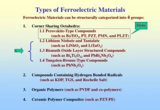
In a DRAM cell capacitor a linear dielectric is used whereas in a FeRAM cell capacitor the dielectric structure includes ferroelectric material, typically lead zirconate titanate (PZT). • A ferroelectric material has a nonlinear relationship between the applied electric field and the apparent stored charge. Lead Zirconate Titanate (PZT) • The dielectric constant of a ferroelectric is typically much higher than that of a linear dielectric because of the effects of semi-permanent electric dipoles formed in the crystal structure of the ferroelectric material. When an external electric field is applied across a dielectric, the dipoles tend to align themselves with the field direction, produced by small shifts in the positions of atoms and shifts in the distributions of electronic charge in the crystal structure.
In the figure a "1" is encoded using the negative remnant polarization "-Pr", and a "0" is encoded using the positive remnant polarization "+Pr".
Writing is accomplished by applying a field across the ferroelectric layer by charging the plates on either side of it, forcing the atoms inside into the "up" or "down" orientation (depending on the polarity of the charge), thereby storing a "1" or "0". Reading the transistor forces the cell into a particular state, say "0". If the cell already held a "0", nothing will happen in the output lines. If the cell held a "1", the re-orientation of the atoms in the film will cause a brief pulse of current in the output as they push electrons out of the metal on the "down" side. The presence of this pulse means the cell held a "1". Since this process overwrites the cell, reading FeRAM is a destructive process, and requires the cell to be re-written if it was changed. WORKING
DENSITY Smaller components, and less of them, means that more cells can be packed onto a single chip, which in turn means more can be produced at once from a single silicon wafer. This improves yield, which is directly related to cost. The lower limit to this scaling process is an important point of comparison, generally the technology that scales to the smallest cell size will end up being the least expensive per bit. FeRAM and DRAM are constructionally similar, and can generally be built on similar lines at similar sizes. In both cases the lower limit seems to be defined by the amount of charge needed to trigger the sense amplifiers. An additional limitation on size is that materials tend to stop being ferroelectric when they are too small. COMPARISON WITH dram SYSTEMS
In DRAM, the charge deposited on the metal plates leaks across the insulating layer and the control transistor, and disappears. In order for a DRAM to store data for anything other than a microscopic time, every cell must be periodically read and then re-written, a process known as refresh. Each cell must be refreshed many times every second (~65 ms) and this requires a continuous supply of power. In contrast, FeRAM only requires power when actually reading or writing a cell. The vast majority of power used in DRAM is used for refresh, indicating power usage about 99% lower than DRAM. Another non-volatile memory type is Flash RAM, and like FeRAM it does not require a refresh process. Flash works by pushing electrons across a high-quality insulating barrier where they get "stuck" on one terminal of a transistor. Power consumption
DRAM speed is limited by the speed at which the current stored in the cells can be drained (for reading) or stored (for writing). FeRAM is based on the physical movement of atoms in response to an external field, which happens to be extremely fast, settling in about 1ns. In theory, this means that FeRAM could be much faster than DRAM. Flash memories commonly need about 1ms to write a bit, whereas even current FeRAMs are at least 100 times that speed. SPEED
A decrease of the remanant polarization reduces the difference between switching- and non-switching charge • Polarization fatigue (after repeated read-write cycles) • Retention loss (with time) • Imprint • shift of the hysteresis loop leads to preference of one polarization state (write failure; only critical at low voltage) or loss of polarization (read failure) • Increase of temperature leads to worse material properties (i.e. defect distribution) FAILURE MECHANISMS
Ferroelectricity is a physical property of a material whereby it exhibits a spontaneous electric polarization, the direction of which can be switched between equivalent states by the application of an external electric field. Piezoelectricity is the ability of some materials (notably crystals and certain ceramics, including bone) to generate an electric potential in response to applied mechanical stress. This may take the form of a separation of electric charge across the crystal lattice. The word is derived from the Greek piezein, which means to squeeze or press. Pyroelectricity is the ability of certain materials to generate an electrical potential when they are heated or cooled. As a result of this change in temperature, positive and negative charges move to opposite ends through migration (i.e. the material becomes polarized) and hence, an electrical potential is established. TECHNOLOGY USED
Magneto resistive RAM Magneto resistive Random Access Memory (MRAM) is a non-volatile computer memory (NVRAM) technology, which has been under development since the 1990s. The advantages are so overwhelming that MRAM will eventually become dominant for all types of memory, becoming a true "universal memory". In MRAM data is not stored as electric charge or current flows, but by magnetic storage elements. Phase Change RAM Phase-change memory (also known as PCM, PRAM, PCRAM, and Chalcogenide RAM C-RAM) is a type of non-volatile computer memory. PRAM uses the unique behavior of chalcogenide glass, which can be "switched" between two states, crystalline and amorphous, with the application of heat. Recent versions can achieve two additional distinct states, effectively doubling its storage capacity. PRAM is one of a number of new memory technologies that are attempting to compete in the non-volatile role with the almost universal Flash memory. FUTURE ENHANCEMENT
Programmable metallization cell The programmable metallization cell, or PMC, is a new form of non-volatile computer memory being developed at Arizona State University and its spinoff, Axon Technologies. PMC is one of a number of technologies that are being developed to replace the widely used flash memory, providing a combination of longer lifetimes, lower power, and better memory density. Silicon-Oxide-Nitride-Oxide-Silicon(SONOS) SONOS, short for Silicon-Oxide-Nitride-Oxide-Silicon, is a type of high-performance non-volatile computer memory. It is similar to the widely used Flash RAM, but offers lower power usage and a somewhat longer lifetime. SONOS is being developed as one of a number of potential Flash replacements, and is currently used in Cypress Semiconductor's PsoC line of products. FUTURE ENHANCEMENT
Resistive random-access memory Resistive random-access memory (RRAM) is a new non-volatile memory type being developed by Fujitsu, Sharp, Samsung, Micron Technology, Spansion, Macronix, Winbond, Unity Semiconductor, and other companies. Racetrack Memory IBM Racetrack Memory is an experimental non-volatile memory device under development at IBM's Almaden Research Center by a team led by Stuart Parkin. In early 2008 a 3-bit version was successfully demonstrated. Developed successfully, racetrack would offer storage density higher than comparable solid-state memory devices like Flash RAM and similar to conventional disk drives, but with much higher read/write performance. It is one of a number of new technologies vying to become a "universal memory" in the future. FUTURE ENHANCEMENT
Nano-RAM Nano-RAM is a proprietary computer memory technology from the company Nantero. It is a type of nonvolatile random access memory based on the mechanical position of carbon nanotubes deposited on a chip-like substrate. In theory the small size of the nanotubes allows for very high density memories. Nantero also refers to it as NRAM in short. FUTURE ENHANCEMENT
FeRAM advantages include: lower power usage, faster write speed and a much greater maximum number (exceeding 1016 for 3.3 V devices) of write-erase cycles. FeRAM disadvantages are: much lower storage densities than Flash devices, storage capacity limitations and higher cost. ADVANTAGES & DISADVANTAGES
FeRAM remains a relatively small part of the overall semiconductor market. Flash memory is produced using semiconductor line widths of 30 nm at Samsung (2007) while FeRAMs are produced in line widths of 350 nm at Fujitsu and 130 nm at Texas Instruments (2007). The areal bit densities of flash memory are consequently much higher than FeRAM, and thus the cost per bit of flash memory is orders of magnitude cheaper than FeRAM. CONCLUSION


![FERROELECTRIC RAM [FRAM]](https://cdn1.slideserve.com/1817127/ferroelectric-ram-fram-dt.jpg)
