R&D on Front-End Electronics for Linear Collider Detector Applications
640 likes | 809 Views
R&D on Front-End Electronics for Linear Collider Detector Applications. Bruce Schumm LECC2004 Workshop Boston, Mass. September 13, 2004. TESLA. Principle 1: The Linear Collider is not the LHC.

R&D on Front-End Electronics for Linear Collider Detector Applications
E N D
Presentation Transcript
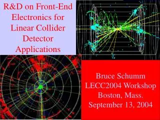
R&D on Front-End Electronics for Linear Collider Detector Applications Bruce Schumm LECC2004 Workshop Boston, Mass. September 13, 2004
TESLA Principle 1: The Linear Collider is not the LHC. What the LC lacks in brute-force discovery reach, it must make up with finesse the LC requires a precision de-tector, and the electronics to instrument it. To understand the need for R&D on front-end electronics for the Linear Collider, it is essential to consider the physics one wants to do.
By the way… the time frame for this R&D is surprisingly current Jae Yu, UT Arlington
e- W/Z W- W+ W/Z e+ Linear Collider Physics Given what we have discovered so far, for high enough energy, this process will happen with greater than unit probability. Our current understanding is incomplete! We need some-thing new to put in the circle. Here are some thoughts…
- + Z0 Haijun Yang, Michigan Mrec for p/ p2= 3x10⁻⁵ THE HIGGS (h0) LC Physics demands precise tracking (Solid state) Mass Recoiling against Z0 Precision demands state-of-the-art central tracker resolution (Gaseous)
The LC must do more than just confirm LHC’s Higgs discovery. It must probe Higgs properties with the precision needed to detect subtle new physics scenarios (SUSY, Little Higgs, etc.) Model-independent branching fractions re-quire unprecedented bot-tom and charm tagging ultraprecise three-dimensional vertexing
e- W/Z W- W+ W/Z e+ If Higgs is just a fairy tale, then more exotic states must play a role ‘Strong WW Scattering’ Henri Videau; Ecole Polytechnique Essential final-state discrimination must be done calorimet-rically ‘Energy-flow reconstruction’places demands on calorimeter design
Timing is Important Pileup of → hadrons for ~200 beam crossings T. Barklow Timing in Cal and Tracking Systems needs to be considered Pileup from 192 crossings (56 Hadronic Events) Pileup from 3 crossings
So… what do we mean by ‘timing’? The Technology Choice Duty Cycle: 5x10⁻³ WARM: Short, intense spill (192 pulses separated by 1.4 ns), and often (120 Hz) COLD: Relaxed but persistent spill (2820 pulses separated by 337 ns); occasional (5 Hz) COLD And the choice is…
The Energy-Flow Concept • Photons and high-energy electrons measured best with calorimetry (ECAL) • Charged hadrons measured best in tracker • Separate clusters in calorimeter and decide what to hand back to tracker HCAL ECAL Requires ‘tracking calorimeter’ with minimal shower spread and maximal segmentation (Moliere radius of W is about 1 cm)
The SD Si/W Group M. Breidenbach, D. Freytag, N. Graf, G. Haller, O. Milgrome Stanford Linear Accelerator Center R. Frey, D. Strom U. Oregon V. Radeka Brookhaven National Lab CALICE is a consortium of 28 institutions from 8 nations
(TESLA TDR) • Proposal for ECAL: • Thin Si diodes read out showers in W layers (Si/W) • Read out each layer with gran-ularity given by Rmoliere (1 cm2) Challenge: This implies a few 107 channels
2 calibration switches chips 6 calibration channels per chip 18 diodes per calibration channel 6 active wafers Made of 36 silicon PIN diodes • 216 channels per board Each diode is a 1cm² square Line buffers To DAQ part Differential 12 FLC_PHY3 front-end chip 18 channels per chip 13 bit dynamic range Presentation of the front-end electronic (J. Fleury, LAL Orsay) 14 layers 2.1 mm thick Made in korea
(J. Fleury, LAL Orsay) Process: 0.8 m BiCMOS
FLC-PHY3 Chip (LAL Orsay) Based on blocks from OPERA HPD readout ASIC Serial Noise (ENC) Linearity At ~200 nsec, Cdet in pF: ENC = 1720 + 28*Cdet (x1 gain) ENC = 950 + 34*Cdet (x10 gain) Now available for instru-mentation of CALICE ECAL prototype (~2000 packages)
Threads in ongoing ECAL front-end electronics Research and Development • For precision calorimetry, compactness is important • Maintain Moliere redius • Calorimetry inside coil • Handle staggering channel count • Multi-channel electronics integrated into detector volume • Power cycling to avoid active cooling • Zero-suppression, timing to avoid pile-up
(R. Frey, SD Si/W group) SD Si/W Ecal Concept
Wafer and readout chip (R. Frey, SD Si/W group)
SD Si/W ASIC • Capacitance • Pixels: 5.7 pF • Traces and pre-amp: 22 pF • Resistance • 300 ohm max • Power • < 40 mW/wafer power cycling • (An important LC feature!) • Signal Processing • Provide fully digitized, zero suppressed outputs of Q and T • One ASIC per wafer • Signals • <2000 e noise • Require MIPs with S/N > 7 • Max. signal 2500 MIPs (5mm pixels) • Dynamically switched Cf • Signals after 1st stage larger • 0.1 mV → 6.4mV for MIP • Much reduced power • Large currents in 1st stage only CALICE will pursue similar development
Hadronic Calorimeter (HCAL) • Need to maintain longitudinal and transverse segmentation: • 5x5 cm2 ‘Analog HCAL’ • 3x3 cm2 ‘Semi-digital HCAL’ • 1x1 cm2 ‘Digital HCAL’ Moscow Engineering and Physics Institute Silicon Photomul-tiplier (SiPM) Ganged Geiger-mode pixels
SiPM Electronics Development • SiPM signals: • gain 106: 1 photo electron = 160 fC • MIPs ~ 25 p.e. = 4 pC • dyn range: Max signal = 400 pC • fast: few ns rise time • pulse shape set by wavelength shifter fiber QE (%) Quantum Efficiency similar to PMT, but single-stage gain, so better statistically than PMT or APD (single-PE statistics) • SiPM noise: • 2MHz noise rate (signal every 500ns) • dominated by 1 pixel signals • necessary calibration signal • But could pile up with slow shaping
Felix Sefkow, DESY SiPM calibration Single photoelectrons • The MIP signal determines the energy scale • monitor overall response • scint, SiPM, FEE • LED: inject UV into scintillator: • Single photon peak spacing • non-linearitycorrection (together with MIP and universal response function) • gain monitoring: SiPM temperature sensitivity: Gain: 3%/K, Signal: 4%/K • Medium LED signals: stability between MIP calibration runs • Large LED signals: direct non-linearity monitoring • Charge injection: electronics calibration a must! MIP Linearity
3.5kΩ 5pF + - 7kΩ 11pF 5.5pF 2.8kΩ Calib switch - + Vref Gm=1uA/V OTA Two Shaping-Time/Two Gain Solution Unipolar/Two Gain Solution (avoid overshoot that can lead to single PE pile-up) • Calibration mode (short shaping) • Single photoelectron response • Cf=0.2pF ; τ =12ns • 1 spe = 8.9 mV ; tp=40 ns • Noise : 720 µV rms • Physics mode (longer shaping) • MIP (=16pe) response • Cf=0.4pF ; Rc=5k ; τ =120ns • Gain = 12 mV/MIP ; tp=186ns • Noise = 570 µV rms Both on same prototype ASIC; to be submitted
Pick-up pads Graphite Signal HV Gas Resistive plates ASIC for ‘Digital HCAL’ – 1 cm2 RPC’s 64 inputs with choice of input gains RPCs (streamer and avalanche), GEMs… Triggerless or triggered operation Output: hit pattern and time stamp
Digital HCAL ASIC J. Repond, Argonne Analog circuitry taken from recently built FSSR chip (BTeV) Hit catcher with pos-sibility to mask noisy channels Chip has data indic-ator (essentially a fast OR) 10 MHz Clock Hope to submit by end of 2004
Gaseous Tracking in the Third Millennium A TPC event from STAR at RHIC Tracking in heavy ion collisions is messy, but TPC’s are highly pixellated • For the Linear Collider Detector: • Track densities are actually higher • Baseline performance implies x3 improvement in point resolution • Must avoid excessive material in endcaps (energy flow into forward calorimetry X0(%) v. (deg)
MICROMEGAS Traditional wire-plane readout too course • Micro-Patterned Gas Detectors • Finer segmentation better res-olution • Ion feedback into tracking volume is small if gain is kept low (~102 per layer) GEM
TPC Electronics Issues Low Noise: want to keep gain low to avoid excessive feedback of ions into the drift volume Channel Count: 2mm2 pads (to achieve 100 m resolution) implies > 106 channels; if limited (350 m) transverse diffusion is exploited, would reach 108 Flash ADC: Exploiting longitudinal diffusion (z drift) resolution limit implies ~100 MHz sampling Signal Processing: Zero suppression, buffering, waveform processing, power cycling, etc. to keep electronics compact and material down Begin upgrade of STAR/ALICE FEL or…
Jan Timmermans, Nikhef Readout microMegas detector with 55x55 m2 pixel MediPix chip Clear depiction of ionization path, -ray Optimal for pattern recognition, two-track separation, dE/dX But: Approaches 1010 channels!!
Solid-State Tracking: the ‘Gossamer Tracker’ Concept • What if the only material in the tracker was the minimum necessary thickness of Si? • No support structure • No cooling • No electronics and servicing • Thinner detectors towards lower radius No – pigs can’t fly. But…
Minimum-ionizing for 300mm of silicon is about 24,000 electrons Operating point for 167 cm ladder Simulations suggest that 3 s shaping time allows ladders to be read from end only no electronics servicing.
‘Just’ switch electronics off during these dead periods ~99% power savings; eliminates need for active cooling What about event pile-up in the tracker? Where SNR = signal-to-noise ratio. For = 3 s and SNR = 12, nsec
Gossamer Tracker FEL Characteristics • Need to develop a chip that… • Has low intrinsic noise • Has long (several s) shaping • Can switch power on/off in ~100 s • Analog readout (centroid, dE/dX) • Time stamping and pipeline • Complementary efforts at: • LPNHE Paris • UCSC (SCIPP) • Both targeting fall prototype run • for example…
RMS RMS Gaussian Fit Gaussian Fit Resolution (10-5 m) Resolution (10-5 m) 167 cm ladder 132 cm ladder
128 mip 0.29 mip threshold 1 mip ¼ mip Response to signals between ¼ and 128 mips (in factor-of-two octaves)
Power On Power Off 60 sec power restoration 8 msec power-off period (not to scale) Response to ¼, 1 and 4 mip signals
Global Baseline LC Vertex Detector Optimistic projections achieved by very small (~20m x 20m) pixels and very thin (<0.1% X0) layers Thinned CCD’s 10 m 5 m Best yet (SLD) Proposed 1 m
But: transition from SLC to LC application is not immediate… Typical CCD sensor includes roughly ¼ million pixels and takes ~100msec to read out with a 5 MHz clock For the LC, this would integrate over the full train of 2,820 pulses, leading to intractable backgrounds Speed up and de-serialize readout Column-parallel CCD readout architecture
Column-parallel CCD has been developed (E2V corporation) Readout scenarios under development
Readout Chip CPR1 6 mm Wire/bump bond pads ASIC for CPC-1 readout • design: RAL Microelectronics Group • voltage amplifiers for 1-stage SF outputs • charge amplifiers for direct outputs • 20 μm pitch, 0.25 μm CMOS process • wire- and bump-bondable • scalable and designed to work at 50 MHz Charge Amplifiers Voltage Amplifiers Voltage Amplifiers Charge Amplifiers 250 5-bit flash ADCs 250 5-bit flash ADCs 6.5 mm 250(W)132(L)5-bit FIFO 250(W)132(L)5-bit FIFO Wire/bump bond pads
bump bonding performed by VTT (Finland) • connecting to CCD channels at effective pitch of 20mm possible by staggering of solder bumps Spectrum (55Fe) observed from voltage output (less aggressive) nodes; beginning to look promising
BUT: in order to avoid event pile-up, you must read out the detector (many times over!) during the spill… Chris Damerell, Rutherford Labs (LCWS04)
Store charge in 20 slices during ~1sec spill; read out between spills But is there a Plan B??!!
Progress in Active Pixel R&D `Monolithic’ designs (electronics deposited directly onto sensors) – why? • Typical current active pixel detector: • Large-pitch pixel sensor (~100 m or more) • Readout circuitry with fill-factor ~1 • Bump bonds • Servicing and cooling • Does not achieve ideal impact parameter resolution due to pitch and material burden • A number of different approaches are being explored… • MAPS (Monolithic Active Pixel Sensor) • FAPS (Flexible Active Pixel Sensor) • DEPFET (Depleted Field Effect Transistor) APS • SOI (Silicon on Insulator) APS
