Interconnect Working Group
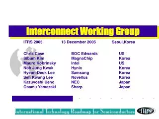
Interconnect Working Group. 2006 Update 5 December 2006 Hsinchu, Taiwan Sam Yamazaki. ITWG Regional Chairs. Taiwan Douglas CH Yu Korea Hyeon-Deok Lee Sibum Kim Japan Tomoji Nakamura Hideki Shibata. US Christopher Case Robert Geffken Europe Hans-Joachim Barth

Interconnect Working Group
E N D
Presentation Transcript
Interconnect Working Group 2006 Update 5 December 2006 Hsinchu, Taiwan Sam Yamazaki
ITWG Regional Chairs Taiwan Douglas CH Yu Korea Hyeon-Deok Lee Sibum Kim Japan Tomoji Nakamura Hideki Shibata US Christopher Case Robert Geffken Europe Hans-Joachim Barth Alexis Farcy
Christopher Case Robert Geffken Hans-Joachim Barth Alexis Farcy Harold Hosack Paul Feeney Ken Monnig Rick Reidy Mauro Kobrinsky Hideki Shibata Kazuyoshi Ueno Michele Stucchi Susan Vitkavage Eiichi Nishimura Mandeep Bamal Bau-Tong Dai Yung-Cheng Lu Anthony Oates Douglas C.H. Yu Lucile Arnaud JD Luttmer Manfred Engelhardt Dirk Gravesteijn NS Nagaraj Mike Mills Skip Berry Gunther Schindler Chung-Liang Chang Tomoji Nakamura Greg Smith Detlef Weber Jin-Ying Song Wen-Jiun Liu Jason Su Hiroshi Miyazaki Shuhei Amakawa Osamu Yamazaki Partial List of Contributors
Agenda • Scope and structure • Technology requirements • Difficult challenges • Cu resistivity effects • Energy and performance • Low k roadmap • Emerging interconnect • Last words
Interconnect scope • Conductors and dielectrics • Starts at conductor etch • Metal 1 through global levels • Includes the pre-metal dielectric (PMD) • Associated planarization • Necessary etch, strip and cleans • Embedded passives • Reliability and system and performance issues • Ends at the top wiring bond pads • Predominantly “needs” based, with some important exceptions (k and resistivity)
Technology Requirements • Tables for HP MPU and ASIC plus DRAM • Wiring levels including “optional levels” • Reliability metrics • Minimum wiring/via pitches by level • Performance figure of merit (Power Index)and capacitance(NEW) • Planarization requirements • Conductor resistivity with and without scattering • Barrier thickness • Dielectric metrics includingeffective k (UPDATED) • Crosstalk metric • Metal 1 variability due to CD and scattering
Difficult challenges • Identify solutions which address wiring scaling issues • Introduction of new materials to meet conductivity requirements and reduce the dielectric permittivity • Engineering manufacturable interconnect structures compatible with new materials and processes
Size matters • 2003 – the impending impact of Cu resistivity increases at reduced feature sizes (due to scattering) - first noted • 2004 – metrics introduced to highlight the impact of width dependent scattering on the effective resistivity and impact on RC delay • Models have been refined to more accurately predict the resistivity due to changes in aspect ratio, shape and metal thickness • 2006 - Metrics have been updated • Adapt the same methodology
Size matters Figure From Infineon For DRAM, Cu is introduced in 2007
Dynamic Power • Increasing concern about rising dynamic power in the interconnect stack • Interconnects make a significant contribution to total dynamic power • Impacts effective k roadmap • Drives reduction in parasitic capacitance • Dynamic power is a key constraint for high performance MPUs NEW
M1IntermediateGlobal upper value P (W/GHz-cm2) C (pF/cm) lower value Used lowest expected k value 90 65 45 32 22 16 M1 ½ pitch 90 65 45 32 22 16 M1 ½ pitch Capacitance and Power Index Capacitance decreases Dynamic power increases NEW
Row to be added to table 80a (“MPU and ASIC Interconnect Technology Requirements—Near-term Years”) shown in red Row to be added to table 80b (“MPU and ASIC Interconnect Technology Requirements—Long-term Years”) shown in red FOOTNOTE TO BE ADDED AT THE BOTTOM OF TABLES 80 (a and b) [x] Power index = C Vdd2 a (1 GHz) ew (1 cm2)/p; p = pitch; Vdd = supply voltage; ew = wiring efficiency = 1/3; a = activity factor = 0.03. The calculated values are an approximation for the “power per GHz per cm2 of metallization layer”. This index scales with the critical parameters that determine the interconnect dynamic power. NOTES: the values provided are an average for M1, Intermediate and Global interconnects. The range of values results from the maximum and minimum effective dielectric constants. NEW
Row to be added to table 80a (“MPU and ASIC Interconnect Technology Requirements—Near-term Years”) shown in red Row to be added to table 80b (“MPU and ASIC Interconnect Technology Requirements—Long-term Years”) shown in red NEW
R and C Variability w=80nm t =70nm w=80nm t =150nm w=100nm t =200nm w=250nm t =200nm Work in progress
Low k again! HP MPU and ASIC Was Is Realistic case in 2007 Aggressive case in 2007 UPDATED
IO - Memory IF & Chip-to-Chip IF - Main Processor DPE DPE DPE DPE DPE DPE DPE DPE Main Processor DPE DPE DPE DPE DPE DPE DPE DPE Multi-core Impact on Interconnect • Wiring lengths change • Critical path reduced (in core) • Mechanical integrity challenges will change • Jmax changes • Hierarchical structure may no longer be necessary • Converge to more fine pitch local/intermediate wires • Power and ground delivered through grid • Global delay challenge relaxed • 3D may include multi-core • Need to consider splitting metrics into: • In-core (intra-tile) and Inter-core (inter-tile) • New bandwidth requirements Figure From ITRS 2006 Design TWG WORK IN PROGRESS
Emerging interconnect • Use geometry • Air gap • 3D • Use different physics • Optics (waveguides, emitters, detectors, free space, trans-impedance amps, modulators) • RF/microwaves (transmitters, receivers, free space, waveguides) • Terahertz photonics • Radical solutions • Nanowires/nanotubes • Molecules • Spintronics • Quantum wave functions WORK IN PROGRESS
From low k to no k - air gaps • Introduction of air gap architectures • Creation of air gaps with non-conformal deposition • Removal of sacrificial materials after multi-level interconnects • Values of effective k-value down to 1.7 with low crosstalk levels • Localized air gaps to maintain good thermal and mechanical properties Ultra-low k and Air gap (k<2.0) (CVD & Spin-on) WORK IN PROGRESS
3D Integration – first thoughts • Through silicon via (TSV) • Reliability • Physical metrics (pitch, diameter, density) • Alignment tolerance • Bond layer • Reliability • Interfacial defect density • Adhesion • List of “Difficult Challenges”, e.g. TSV processes, alignment, low k impact on TSV, etc. Figure From Stanford WORK IN PROGRESS
Last words • Must manage the power envelope • Develop solutions for emerging devices • Must manage 3D-CD • System level solutions must be accelerated to address the wire scaling grand challenge • Cu resistivity increase impact appears ~2006 • materials solutions alone cannot deliver performance - end of traditional scaling • integrated system approach required

