Global Trends in Interconnect Technology at SEMICON Makuhari 2010
The Interconnect Working Group convened at SEMICON Makuhari, Japan on December 3, 2010, focusing on advancements in interconnect technology and materials. Key discussions revolved around conductor and dielectric innovations, including pre-metal dielectrics, embedded passives, and challenges posed by scaling. Contributors from various regions shared insights on reliability, system performance, and electrical characteristics in interconnect design. Topics such as air gap architecture, non-traditional materials, and future projections for contact resistance were highlighted, underscoring the need for a new architecture solution in interconnect systems.

Global Trends in Interconnect Technology at SEMICON Makuhari 2010
E N D
Presentation Transcript
Interconnect Working Group It’s a wired world SEMICON Makuhari, Japan 3 December2010
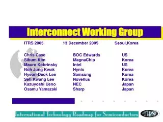
ITWG Regional Chairs Europe Hans-Joachim Barth Alexis Farcy Korea G.H. Choi US Christopher Case Japan Tomo Nakamura Hideki Shibata Taiwan Douglas CH Yu
Partial List of Contributors ShuheiAmakawa Nobuo Aoi SitaramArkalgud Lucile Arnaud Koji Ban Hans-Joachim Barth Eric Beyne Christopher Case Chung-Liang Chang Hsien-Wei Chen GilheyunChoi Jinn-P. Chu Mike Corbett Alexis Farcy Paul Feeney Masayuki Hiroi Masayoshi Imai Raymond Jao Shin-PuuJeng Sibum Kim Mauro Kobrinsky NohjungKwak HyeonDeok Lee Scott List Anderson Liu Didier Louis Toshiro Maekawa Akira Matsumoto Azad Naeemi NS Nagaraj Tomoji Nakamura Yuichi Nakao • Akira Ouchi • Peter Ramm • Rick Reidy • Scott Pozder • Philip Pieters • Andy Rudack • Larry Smith • Mark Scannell • Hideki Shibata • Michele Stucchi • Wen-ChihChiou • Weng Hong Teh • Thomas Toms • Manabu Tsujimura • Kazuyoshi Ueno • Osamu Yamazaki • 1210
Interconnect scope Conductors and dielectrics Starts at contacts Metal 1 through global levels Includes the pre-metal dielectric (PMD) Associated planarization Necessary etch, strip and cleans Embedded passives Global and intermediate TSVs for 3D Reliability and system and performance issues “Needs” based replaced by – scaled, equivalently scaled or functional diversity drivers.
Hierarchical Cross Sections Wire Wire Wire Via Via Via Metal 1 Pitch Metal 1 Pitch Passivation Dielectric Etch Stop Layer Global (=IMx1.5~2µm) Dielectric Capping Layer Global (=IMx1.5~2µm) Copper Conductor with Barrier / Nucleation Layer Semi- Global (=M1x2) Inter- Mediate (=M1x1) Inter- Mediate (=M1x1) Metal 1 Tungsten Contact Plug Metal 1 • MPU : Revised hierarchy • ASIC : No drastic change, however semi-global should be kept at 2 x M1 Pre-Metal Dielectric ASIC Cross-Section MPU Cross-Section
Technology Requirements Now restated and organized as General requirements Resistivity Dielectric constant Metal levels Reliability metrics Level specific requirements (M1, intermediate, global) Geometrical Via size and aspect ratio Barrier/cladding thickness Planarization specs Materials requirements Conductor effective resistivity and scattering effects Electrical characteristics Delay, capacitance, crosstalk, power index
Difficult challenges (1 of 2) Meeting the requirements of scaled metal/dielectric systems Managing RC delay and power New dielectrics (including air gap) Controlling conductivity (liners and scattering) Filling small features Barriers and nucleation layer Conductor deposition Reliability Electrical and thermo-mechanical Engineering a manufacturable interconnect stack compatible with new materials and processes Defects Metrology Variability
Difficult challenges (2 of 2) Meeting the requirements with equivalent scaling Interconnect design and architecture (includes multi-core benefits) Alternative metal/dielectric assemblies 3D with TSV Interconnects beyond metal/dielectrics 3D Optical wiring CNT/Graphene Reliability Electrical and thermo-mechanical Engineering a CMOS-compatible manufacturable interconnect system Non-traditional materials (for optical, CNT etc.) Unique metrology (alignment, chirality measurements, turning radius etc)
HistoricalTransitionofITRSLow-kRoadmap Since 2003, based on wiring capacitance calculation of three kinds of dielectric structures and validated against publications ITRS2003 ITRS2005 ITRS2007-2010 Effective Dielectric Constant; keff ITRS2001 Before 2001, unreasonable RM without logical basis ITRS1999 Year of 1st Shipment 2009 decreased max bulk k by 0.1 - no significant change on keffin 2009 2010 no changes 2009 Summer Conference
2010 Low k or nothing? • Air gap architectures will be required forkbulk<2.0 • No viable materials expected to be available. • Mechanical requirements easier to achieve with air-gaps. • End of the material solution and the beginning of an architecture solution.
Air Gap • Approaches • Creation of air gaps with non-conformal deposition • Removal of sacrificial materials after multi-level interconnects Pictures (top left, clockwise): NXP, IBM, TSMC, Intel, Panasonic.
2010 Barrier/Nucleation/Resistivity • Barrier layer requires an appropriate combination of liners and nucleation layers potentially with ALD, and considering low k properties. • Resistivity increases due to scattering and impact of liners • -No known practical solutions
Cu Contact Transition Prospective • 5% of total parasitic resistance for contact resistance (agreed with PIDS, FEP and INTC in 2008) • Estimation of contact resistance used to forecast timing for Cu ITRS 65~54nm 45~32nm 27~21nm 19nm~ 45/40nm 32/28nm 22/20nm 15nm Commercial W-plugwill be applicable until 22/20nm node at 2013. 200 NG Target W-plug 150 Cu-plug Cu-plug will be able to satisfy the requirement beyond 15/14nm node after 2016. Resistance (/contact) 100 marginal • Assumption • Aspect ratio=5.5 • Barrier for W-plug • PVD-Ti 10nm@btm, 2nm@side • CVD-TiN5nm@btm/side • Barrier for Cu-plug • PVD-Ta(X)5nm@btm, 1nm@side • CVD-Ru(X) 2nm@btm/side 50 OK 0 2007 2010 2013 2016 Year
Wire current limit – width dependence The color boundaries may actually be width-dependent. Hu et al., Microelectronics Reliability, vol.46, pp.213-231, 2006. Jmax will increase with frequency and reducing cross-section, while JEM will scale with the product w*h according to EM lifetime dependence on wiring width Jmax 2007 Jmax 2008 2008 Update 2010 revised Jmax JEM Year
Metal Capping <CoWP-Cap> CuSi(N) + Ti-BM CuAl <CuSiN-Cap> CuSiN(2) Si Si Si Si Si Si Si CoWP Si Si Si Si Si EM Lifetime Improvement Ratio Si <CuAl-Alloy> <CuGeN-Cap> CuSiN(1) CuSiN Ge Ge Ge Ge CuGeN Al Al Al Al Al Al Al Al Al Al Al Al Al Al Al Al Normalized Resistance Increase Ratio <CuSiN-Cap+Ti> Various lifetime improvement approaches against the resistivity increase H. Shibata added published data based on Yokogawa et. Al. IEEE Trans on ED.2008
High Density TSV Roadmap or“enabling terabits/sec at femtojoules/bit” The Interconnect perspective - examples: High bandwidth/low energy interfaces between memory and logic Heterogeneous integration with minimal parasitics (analog/digital, mixed substrate materials, etc.) “Re-architect” chip by placing macros (functional units) on multiple tiers (wafers) and connect using HD TSVs Defined a 3D interconnect hierarchy TSV dimensions Minimum contact pitches Overlay accuracy Described process modules
Emerging Interconnect Changes OUT: • Air gaps Process Module Section • Increasing maturity of integrated air gap solutions • 3D Process Module and Architecture Sections • 3D with TSVs nearing production IN: • Focus on Cu Replacements • Section on Native Device Interconnects • Identified need to jointly consider switch and interconnect properties of new switch options
Emerging Interconnect Summary Table • Interconnect options include Cu Extensions, Cu Replacements and Native Device Interconnects ~Example of Approaches for Cu Replacements ~
Native Device Interconnects GNRs (ballistic) Nanowires (ballistic) 12kW 1kW/µm • Doped NWs require silicidation for lengths > 1µm • Multi-fanouts are easy • Multi-layer routability incurs quantum resistance Spin Waves CNTs (ballistic) 1 MW l mfp • Multi-fanouts are very difficult • Serial, multi-input AND gates are easy • Diffusion and spin wave transport are 1000 times slower than electron transport • Spin relaxation lengths are ~ 1µm
Potential interconnect state variables GA Tech is using a Benchmarking Approach: Define possible transportation mechanisms in general Model delay and energy per bit for various transport mechanisms. Benchmark new state variables against their conventional counterpart as a function interconnect length. From Naeemi et al.
Delay versus Length Diffusion Spin Waves (104 m/s) CMOS (Min-Size Driver) Spin Waves (105 m/s) Two spin wave phase velocities of 104 (realistic) and 105 m/s (optimistic) are considered. Driver delay is not included for new state variables (upper bound performance) Delay (ps) Ballistic CMOS (5x Driver) Drift Interconnect Length (Gate Pitch) • Communications of new state variables are all slow compared to conventional CMOS interconnects.
Energy per bit DRIFT,0.8V CMOS DIFFUSION SWB For a Co30Fe70 SWB, energy is taken to be 1aJ/um* • The excitation energy has been optimistically assumed to be negligible. * A. Khitun et al, Nanotechnology, vol. 18, no. 46, 2007.
Formidable Task: Fabricating Dense Bundles of SWNTs • Fabricating bundles of densely packed SWNTs in the horizontal plane for interconnects has proven very challenging. • Making contacts to horizontal bundles of SWNTs is very difficult. • Promising progress in creating aligned isolated SWNTs by transferring SWNTs grown on sapphire to other substrates. • Single SWNTs are too resistive for general purpose CMOS circuits. Young Lae Kim et al. (RPI, RICE & NorthEastern Univ Y. Nishi and H.-S. Philip Wong (Stanford)
Graphene – a “Nobel Prize” winning interconnect option beyond Cu/Low k? • Graphene Potentials • Device/interconnect synergism • Tunable bandgap • Ballistic transport for > 10 mm • Planar technology • Excellent Jmax • Potential CVD deposition process • Graphene Areas for Research • Layer to layer coupling/scattering • Low T CVD deposition • Effective bandgap control • Contact resistance/reliability
Native Device Interconnect Prognosis • Interconnects can impose major limits on both charge and non-charge based devices. • Most transport mechanisms for novel state-variables are relatively slow. • The new devices must offer better delay-energy trade-offs compared with conventional CMOS devices. • Interconnects have important implications at the device, circuit and architecture levels.
Interconnect Summary 2010 3D and air gaps moved out of emerging sections Low-k – unchanged – second time in 10 years Air gaps expected to be solution for kbulk <2.0 Accelerated in 2011 with kbulk <2.4 Jmax current limits are width dependent - a new concern Barriers and nucleation layers are a critical challenge ALD integration is still being investigated including the combination with appropriate dielectrics and barrier metals. Approaches of new liners (Co, Ru and others) stacked with barrier layers are proliferating Capping metal for reliability improvement New interconnect 3D TSV roadmap tables Cu contact need expected >2013 Emerging interconnect solutions are being developed First principle consideration for native interconnects to distinguish interconnect from switching properties of emerging devices and materials– CNT, graphene, nanowires etc. - 28 - - 28 -