CPU Controller Design: System Block Diagram & Control Signals
60 likes | 130 Views
Design a CPU controller with sequential controller and combinational ALU control using Verilog, testing with memory modification and program execution at location 0.

CPU Controller Design: System Block Diagram & Control Signals
E N D
Presentation Transcript
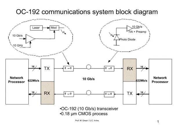
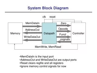
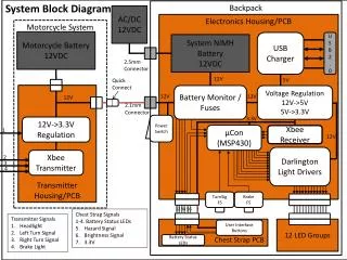
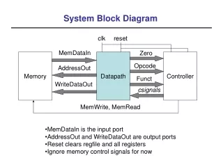
System Block Diagram clk reset MemDataIn Zero Memory Datapath Controller Opcode AddressOut Funct WriteDataOut csignals MemWrite, MemRead • MemDataIn is the input port • AddressOut and WriteDataOut are output ports • Reset clears regfile and all registers • Ignore memory control signals for now
Program Execution • Only two system inputs, reset and clock • Reset zeroes out all registers • Sets PC to first memory address • After reset the program at location 0 should be executed • PC should increment after each instruction (except beq) • Memory must contain program at address 0
Controller Design zero Controller ALU Control aluOP opcode (IR 31-26) funct (IR 5-0) ALU control signals most control signals • Datapath needs new outputs opcode and funct • Controller is sequential, ALU Control is combinational • Reset and clock signals not shown
Main Controller • A big case statement based on the opcode case (opcode) begin 35: cseq_lw(sclk); 43: cseq_sw(sclk); 0: cseq_rtype(sclk); … • Assume a task for each instruction type • Opcodes will be given to you
ALU Control • A big case statement based on ALUOp and funct case (ALUOp) begin 00: ALUcontr = 010; 10: case (funct) begin 32: ALUcontr = 010; … • Assume a task for each instruction type • Opcodes and functs will be given to you
Testing the CPU • Modify the Verilog code of the memory • Write a program starting at location 0 • Reset the machine • Check the results of the program