Download
1 / 64
660 likes | 926 Views
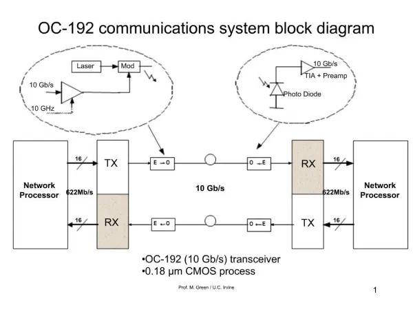
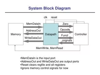
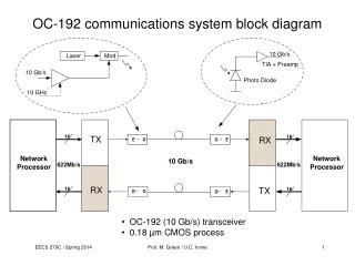
OC-192 communications system block diagram. 10 Gb/s. Laser. Mod. TIA + Preamp. 10 Gb/s. Photo Diode. 10 GHz. 16. 16. TX. RX. E O. O E. Network. Network. 10 Gb/s. 622Mb/s. 622Mb/s. Processor. Processor. RX. TX. 16. 16. E O. O E.

E N D
OC-192 communications system block diagram 10 Gb/s Laser Mod TIA + Preamp 10 Gb/s Photo Diode 10 GHz 16 16 TX RX E O O E Network Network 10 Gb/s 622Mb/s 622Mb/s Processor Processor RX TX 16 16 E O O E • OC-192 (10 Gb/s) transceiver • 0.18 µm CMOS process Prof. M. Green / U.C. Irvine
Transceiver block diagram: 10 GHz 10 Gb/s Prof. M. Green / U.C. Irvine
Transmitter Block Diagram FIFO Control RESET OVF CLK16IP Write Pointer CLK16IN DI0P DI0N 16 X 10 FIFO LVDS Parallel Input Bus INPUT REGISTER TSDP Output Retime 16:1 MUX CML High- Speed Outputs TSDN DI15P TSCKP DI15N TSCKN Read Pointer SELFECB RB_LD LVDS Output Clock REF155EN CLK16OP DIVIDE-BY-16 LVPECL Ref. Clock CLK16ON REFCLKP 10/10.7 GHz CMU REFCLKN LCKDET IFSEL VCP VCN Prof. M. Green / U.C. Irvine
Low-Frequency Input signals Input clock Input data aligned to input clock (usually jittery) Input data T Very low jitter (~10 ppm) reference clock; used in CMU to generate 10 GHz internal clock Reference clock tsh Reference clock and input clock are not synchronized. Maximum allowable variation between Input clock & Reference clock is T − tsh Prof. M. Green / U.C. Irvine
Illustration of Input Timing Regimes Reference clock High-frequency clock input clock 16 16:1 MUX 16 16 input data Input clock timing domain Reference clock timing domain Connection could exhibit varying delay Variable phasing between input & reference clock domains can cause bit errors in MUX Prof. M. Green / U.C. Irvine
First-In/First-Out (FIFO) Circuit (1) 16:1 MUX We require an intermediate block to resolve timing variations between input & reference clock Prof. M. Green / U.C. Irvine
First-In/First-Out Circuit (2) Read clock based on input clock Write clock based on reference clock Read clock Write clock k Din_0 Dout_0 Ref clock Synchronized with input clock Read clock Write clock To serializer (signals synchronized with reference clock) Din_n k Dout_n Ref clock Since these signals have period k times longer than the input period, the circuit can tolerate k times larger variation between input & reference clocks. Prof. M. Green / U.C. Irvine
FIFO approach: • Large amount of hardware (many latches) • Significant power dissipation unless static CMOS is used • Can handle arbitrarily large delay variations Appropriate phase chosen • DLL approach: • Less hardware • Can handle modest delay variations • Better choice for BJT or GaAs processes Prof. M. Green / U.C. Irvine
16:1 Multiplexer Tree Structure 2.5 GHz 1.25 GHz 10 Gb/s 5 GHz 1.25 Gb/s 2.5 Gb/s 5 Gb/s static CMOS CML Prof. M. Green / U.C. Irvine
2:1 MUX cell details D flip-flop with extra latch Prof. M. Green / U.C. Irvine
10ISS 2ISS 5ISS ISS Total current: 18ISS • Assume all blocks have: • Tail current ISS • Resistor R • Diff pair transistor sizes W/L Prof. M. Green / U.C. Irvine
Lower bit rate allows lower power! We can take advantage of gain/bandwidth tradeoff by appropriate scaling: • Design parameters: • ISS • R • W/L CL Idea: Prof. M. Green / U.C. Irvine
Cp ≈ 10 fF GSCALE=3 ISS = 1.2 mA MSCALE=1/8 MSCALE=1/2 MSCALE=1/2 MSCALE=1 Itotal = 5.75ISS = 6.9 mA Prof. M. Green / U.C. Irvine
Clock Dividers The operation of “real” high-speed clock dividers is more complex … Prof. M. Green / U.C. Irvine
Clock divider based on CML D flip-flop: Divider sensitivity curve: Vmin = minimum input clock amplitude required for correct operation. fso = self-oscillation frequency Vmax = maximum dc differential voltage that can be applied to the input clock for which the circuit self-oscillates. Vmax Prof. M. Green / U.C. Irvine
Sensitivity Curve Analysis Desired frequency divider operation Quasiperiodic operation Slew-rate limited operation Region I: Region II: Region III: Prof. M. Green / U.C. Irvine
Region II: Quasiperiodic behavior self-oscillating fin = 11GHz locked Prof. M. Green / U.C. Irvine
Region III: Slew-rate limited Behavior Sine-wave input Square-wave input Prof. M. Green / U.C. Irvine
Effect of Transistor Sizes on Sensitivity Curve Driver transistors Latch transistors Clock transistors Prof. M. Green / U.C. Irvine
Alternatives to DFF-Based Clock Dividers • Latches present large capacitive load slow Prof. M. Green / U.C. Irvine
At very high frequencies, latch transistors are not necessary and only add capacitance to the circuit: Prof. M. Green / U.C. Irvine
Ring-Oscillator-Based Divider Behaves like a 4-stage ring oscillator with injection of full-rate frequency. Prof. M. Green / U.C. Irvine
Comparison of Sensitivity Curves Conventional divider: Dynamic divider: Wider frequency range; lower self-oscillation frequency Narrow frequency range; higher self-oscillation frequency Prof. M. Green / U.C. Irvine
Effect of Non-Ideal Clock Signals I1 I2 Offset resistance causes deviation from 50% duty cycle in clock signal. I2(t) ISS I1(t) 0 Vout-(t) VDD Vout+(t) VDD – ISSR VDD – ISS(R+DR) ISSR 0 ISS(R+DR) Vout+(t)–Vout-(t) Prof. M. Green / U.C. Irvine
Result of nonideal half-rate clock is Periodic Jitter. ideal ideal with offset with offset Half-rate clock MUX output Prof. M. Green / U.C. Irvine
Retimer eliminates this problem: retimer 10 Gb/s data 10 Gb/s retimed data 5 Gb/s 5 GHz 10 GHz clock retimed output Full-rate clock (could be non-50% duty cycle) Prof. M. Green / U.C. Irvine
Internal MUX Timing 10 Gb/s data output 5 Gb/s 2.5 Gb/s data input 2.5 MHz 10 GHz clock 5 GHz tp2 tp1 tp1 & tp2 are “clock-to-Q” delays. Because the clock & data flow in opposite directions, alignment between 5 Gb/s data & 5 GHz clock is determined by the sum: tp1 + tp2 (High sensitivity to processing / temp. corners) Prof. M. Green / U.C. Irvine
Serial Output 50 Line Driver • 50 back termination used to reduce reflections. • CML blocks scaled up so that last stage drives ac load of 25 • Shunt-peaking used in second stage. Prof. M. Green / U.C. Irvine
Receiver Block Diagram Prof. M. Green / U.C. Irvine
DMUX Architecture Prof. M. Green / U.C. Irvine
1:4 DMUX Tree Structure 5 Gb/s 10 Gb/s data input 2.5 Gb/s data outputs 5 GHz 2.5 GHz 10 GHz clock Prof. M. Green / U.C. Irvine
1:2 DMUX cell details: Prof. M. Green / U.C. Irvine
Internal DMUX Timing 5 Gb/s 10 Gb/s data input 2.5 Gb/s data output tp2 5 GHz 2.5 GHz 10 GHz clock tp1 tp1 & tp2 are “clock-to-Q” delays. Because the clock & data flow in the same direction, alignment between 5 Gb/s data & 2.5 GHz clock is determined by the difference: tp1 – tp2 (Low sensitivity to processing/temp. corners) Prof. M. Green / U.C. Irvine
Crosstalk in Transceivers f1 f2 • Capacitive coupling between VCO’s can cause “frequency pulling” • Momentary differences in frequencies between 2 VCO’s can give rise to additional jitter. Prof. M. Green / U.C. Irvine
Crosstalk Measurement CMU reference clock Serial input data 10 Gb/s Low-frequency inputs/outputs Low-frequency inputs/outputs recovered clock 10 GHz output clock 10 GHz + 100ppm output data 10 Gb/s + 100ppm Jitter is measured at TX output clock (or data) and RX recovered clock. Prof. M. Green / U.C. Irvine
Techniques for Reducing Transceiver Crosstalk • Sufficient physical separation between VCO’s • Separate supply connections to package for each block • (e.g., CMU, CDR, MUX, DMUX, FIFO, etc.) • Ample guard rings to minimize substrate coupling Very difficult to simulate & predict! Prof. M. Green / U.C. Irvine
SONET Jitter Specifications • Jitter Generation (transmitters) • Jitter Tolerance (receivers) • Jitter Transfer (repeaters) Prof. M. Green / U.C. Irvine
Jitter Generation (1) Wideband jitter (p-p or rms) can be measured directly from serial output data signal • DJ always specified in peak-to-peak • RJ rms jitter well-characterized • RJ peak-to-peak jitter dependent on measurement time (increases without bound) SONET: JPP usually measured over a specified frequency range. Gigabit Ethernet & Fiber Channel: Equivalent JPP determined by measured BER. Prof. M. Green / U.C. Irvine
Jitter Generation (2) SONET jitter generation is specified within a certain jitter frequency range. For OC-192: 50 kHz – 80 MHz • To measure narrowband jitter generation, we can: • Measure the recovered clock from a “golden” CDR: Ref. clock CDR (low jitter generation) output data TX recovered clock Should have jitter bandwidth > 80MHz 10 GHz SONET OC-192 bandpass filter to jitter analyzer Prof. M. Green / U.C. Irvine
Jitter Generation (3) • Measure the TX output clock directly • (assuming its jitter is the same as the data): Ref. clock output data TX TX output clock 10 GHz to jitter analyzer Note: ISI is usually measured separately (peak-to-peak only). Prof. M. Green / U.C. Irvine
Jitter Generation (4) Measured at output clock; 231-1 PRBS serial data applied to input 9.95328 GHz 10.6642 GHz Phase noise: -100 dBc/Hz @ 1MHz offset Jitter generation (SONET filter): 5.6mUI rms / 60mUI p-p Phase noise: -100 dBc/Hz @ 1MHz offset Jitter generation (SONET filter): 6.2mUI rms / 65mUI p-p Prof. M. Green / U.C. Irvine
Jitter Generation (5) Jitter measurements from clock: Closed-loop VCO phase noise (231-1 PRBS): –107 dBc/Hz @ 1 MHz offset Jitter Generation (231-1 PRBS): 6.44 ps pp (wide band) 0.38ps rms (within SONET band) Prof. M. Green / U.C. Irvine
Jitter Generation (6) 231-1 PRBS input data applied: 10.6642GHz clock Wideband jitter: 7.5ps p-p / 1.2ps rms 10.6642Gb/s data Wideband jitter: 10.7ps p-p / 1.8ps rms Prof. M. Green / U.C. Irvine
Jitter Tolerance (1) Experiment: Apply serial data to CDR with jitter at a certain frequency. Increase the jitter amplitude until a bit error occurs. retimed data out Serial data in To DMUX retimer recovered clock If data jitter & recovered clock jitter could perfectly track, then retiming would be error-free. T Recovered clock tsh Data in Prof. M. Green / U.C. Irvine
Jitter Tolerance (2) ^ Given CDR open-loop characteristic fdata fclock (expressed in UI) Prof. M. Green / U.C. Irvine
Jitter Tolerance (3) 10000 Bit rate: 10.7 Gb/s Pattern: 231-1PRBS Data in: 50 mV pp BER threshold: 10-12 Bit rate: 10.7Gb/s Pattern: 231-1PRBS BER threshold: 10-12 1000 100 Jitter Tolerance [UIpp] 10 1 0.1 0.01 10 100 100M 1K 10K 100K 1M 10M Jitter Frequency [Hz] Jitter Frequency (Hz) Jitter Tolerance > 40 ps pp at high frequency Prof. M. Green / U.C. Irvine
Jitter Transfer repeater RX TX O E E O n repeaters: Jitter peaking should be minimized. Jitter Transfer Mask: 0.1dB -20 dB/decade f0 Prof. M. Green / U.C. Irvine
Electrical-to-Optical Interfaces (1) Electrical to optical (TX): IL MUX laser driver laser diode or Vertical Cavity Surface Emitting Laser (VCSEL) optical output power T IL Prof. M. Green / U.C. Irvine
Electrical-to-Optical Interfaces (2) Pin VM Pout VM Vswing~ 3V Electroabsorption modulator Operates by making optical material more or less absorptive. Prof. M. Green / U.C. Irvine 49
Electrical-to-Optical Interfaces (3) VM Vswing ~ 6V Mach-Zender modulator: Mach-Zender interferometer: • Invented in 1890s • Used to precisely measure optical phase shift of materials. • By using constructive/destructive interference, can be used as a laser modulator. Prof. M. Green / U.C. Irvine 50