Download
1 / 9
100 likes | 265 Views
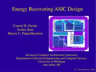
Serializer ASIC design at SMU. Andy Liu on behalf of the SMU group December 6, 2011 LAr Week, CERN. Optical link Overview . On-detector, rad tol. Off-detector, COTS. Trans-impedance amplifiers. VCSELs. Laser drivers. FPGA. ADC Data. TIA. deserializer. Optical fibers. PIN diode.

E N D
Serializer ASIC design at SMU Andy Liu on behalf of the SMU group December 6, 2011 LAr Week, CERN
Optical link Overview On-detector, rad tol Off-detector, COTS Trans-impedance amplifiers VCSELs Laser drivers FPGA ADC Data TIA deserializer Optical fibers PIN diode LD Multiplexers Serializers Optical transmitters Optical receivers Optical Links
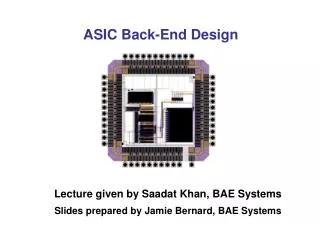
LOCs1 Review 5 Gbps • Process: fabricated in a commercial 0.25 μm Silicon-on-sapphire (SoS) CMOS technology • Input: 16 bit parallel data and 1 clock, LVDS • Output: 1 bit serial, CML • Operation range: 4.0 – 5.7 Gbps • Power dissipation: 463 mW • Radiation tolerant 3 mm TIPP 2011 – 11 June 2011 – Chicago, Illinois 3 mm
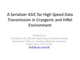
LOCs2 block diagram + Status Liu@SMU • In design: • 2-ch serializers, 8 Gbps/ch • 4-ch VCSEL driver array, 8 bps/ch • Status: • All fast blocks in CML logic done (dark green) • Other parts in light green have been verified in LOCs1, under fine tuning. • Single channel VCSEL driver done, moving to an (open drain) driver array • The LVDS receiver will need to be checked
CML circuits in LOCs2 Liu@SMU The CML Driver has been changed to 5 stages and 3.3V power supply to improve performance in jitter and amplitude. Designed low speed CML divider and CML multiplexer circuits to replace CMOS circuits in Stages 2 and 3 multiplexers to reduce noise and power consumption.
Test the CML circuits Test schematic of all high speed CML circuits Liu@SMU Tested all high speed CML circuits in a test bench shown below. The overall DJ is about 14 ps (p-p) at typical corner 27 C.
The VCSEL driver the schematic of a VCSEL driver (only the last two stages shown) an eye diagram at 8 Gbps (post layout simulation, DJ < 6 ps) Liu@SMU A single channel VCSEL driver operating at 8 Gbps has been designed. A 4-channel VCSEL driver matching a VCSEL array is under development. Will expand to 12 channel once proved successful. Limited by MPW.
Adjustable Active Peaking Liu@SMU Proposed using an external voltage to adjust the peaking strength. The control will be moved inside the chip in the final version (using DAC).
Plan Liu@SMU Initially planned to submit (MPW run) in March 1, 2012, now the designers would like to move that to May 1, 2012. The designers would like to request a review organized by LAr sometime in Jan./Feb. time frame. We have started looking into the packaging issue, together with the array optical transmitter development. Will report next time.