ASIC/FPGA design flow
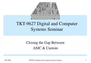
ASIC/FPGA design flow. Design Ideas. Detailed Design. Functional Simulation. Device Programming. Timing Simulation. Synthesis & Implementation. FPGA CPLD. t pd =22.1ns f max =47.1MHz. Design Flow. Design Ideas. Detailed Design. Functional Simulation. Device Programming.


ASIC/FPGA design flow
E N D
Presentation Transcript
Design Ideas Detailed Design Functional Simulation Device Programming Timing Simulation Synthesis & Implementation FPGA CPLD tpd=22.1ns fmax=47.1MHz Design Flow
Design Ideas Detailed Design Functional Simulation Device Programming Timing Simulation Synthesis & Implementation FPGA CPLD tpd=22.1ns fmax=47.1MHz Design Flow
Design Ideas • What are the main design considerations? • Design feasibility? • Design spec? – (UML, C/C++, Behavioral VHDL) • Cost? • FPGA/CPLD or ASIC? • Which FPGA/CPLD vendor? • Which device family? • Development time?
Detailed Design • Choose the design entry method • Schematic • Gate level design • Intuitive & easy to debug • HDL (Hardware Description Language), e.g. Verilog, VHDL, SystemC • Descriptive & portable • Easy to modify • Mixed HDL & schematic • Manage the design hierarchy • Design partitioning • Chip partitioning • Logic partitioning • Use vendor-supplied libraries or parameterized libraries to reduce design time • Create & manage user-created libraries (circuits)
Functional Simulation • Preparation for simulation • Generate simulation patterns • Waveform entry • HDL testbench • Generate simulation netlist • Functional simulation • To verify the functionality of your design only • Simulation results • Waveform display • Text output • Challenge • Sufficient & efficient test patterns
assign z=a&b a z b HDL Synthesis • Synthesis = Translation + Optimization • Translate HDL design files into gate-level netlist • Optimize according to your design constraints • Area constraints • Timing constraints • Power constraints • ... • Main challenges • Learn synthesizable coding style • Write correct & synthesizable HDL design files • Specify reasonable design constraints • Use HDL synthesis tool efficiently
a z b FPGA CPLD 01011... Design Implementation • Implementation flow • Netlist merging, flattening, data base building • Design rule checking • Logic optimization • Block mapping & placement • Net routing • Configuration bitstream generation (FPGA only) • Scan flip-flop insertion (ASIC only) • Implementation results • Design error or warnings • Device utilization • Timing reports • Challenge • How to reach high performance & high utilization implementation?
Timing Simulation (optional) • Post-layout simulation • Includes component and wire delays, clock skew, setup and hold times • Same input vectors with functional simulation • Not necessary if Static Timing Analysis shows no problems
FPGA CPLD Device Programming (FPGA only) • Choose the appropriate configuration scheme • SRAM-based FPGA/CPLD devices • Downloading the bitstream via a download cable • Programming onto a non-volatile memory device & attaching it on the circuit board • OTP, EPROM, EEPROM or Flash-based FPGA/CPLD devices • Using hardware programmer • ISP • Finish the board design • Program the device • Challenge • Board design • System considerations