2 ASIC Design Methodology
2 ASIC Design Methodology. 1) Definition 2) Design Representation(Top-down, B-S-P) 3) Design Objectives 4) ASIC Types 5) ASIC Design Process 6) Cost Analysis. Contents. 1) Definition of ASIC. ASIC is application-specific.

2 ASIC Design Methodology
E N D
Presentation Transcript
2 ASIC Design Methodology 1) Definition 2) Design Representation(Top-down, B-S-P) 3) Design Objectives 4) ASIC Types 5) ASIC Design Process 6) Cost Analysis Contents
1) Definition of ASIC • ASIC is application-specific. (vs. General-Purpose, Commodity or Standard IC i.e., memory, microprocessor) • ASIC can become ASSP(Application-Specific Standard Product) if volume becomes large.(ex:MODEM, disk controller) • ASIC integrates many block in one chip. (Today’s board is tomorrow’s ASIC.)
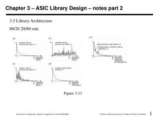
3) Design Objectives low performance FPGA Gate array C BIC NRE Cost Full-custom high long PTAT(Product Turn-around Time) Per-chip cost(chip area) high
4) ASIC Types • PLD PAL(device name), PLA(circuit style) ; all AND-OR plane logic(two-level logic) • FPGA • Gate Array(with or without embedded block, ex;memory) • Standard Cell(w. or w/o macro) • Compiled block ; datapath, RAM, ROM, multiplier • Full - Custom Semi-custom IC (ASIC in narrow sense)
Important elements in ASIC Design System specification in-house CAD tools IP ASIC design library Commercial CAD tools ASIC foundry
The macrocells typically consist of programmable array logic followed by a flip-flop or latch. The macrocells are connected using a large programmable interconnect block. Programmable logic device(PLD) die.
All FPGAs contain a regular structure programmable interconnect. Field-programmable gate array(FPGA) die.
Two-step manufacturing Full-custom fabrication Semi-custom fabrication Standard phase custom phase
Standard & Custom Masks Two-step manufacture : First(deep) processing steps Base wafers Standard masks Custom masks Customization : contacts & metal layers ASIC
Architecture Specifications • Master array = core + I/O pads • Core : - macro-architecture • number & distribution of basic core cells • embedded(specialized) structures - micro-architecture • isolation method : gate or oxide isolation • predefined channels or channelless layout • available devices : transistors, capacitors, resistors, … • NMOS/PMOS transistor count ratio • number of contacts to each transistor gate, source or drain • spacing between transistors, or transistor pitch • identical or variable size transistors • relative size of the NMOS and PMOS transistors • layout of the basic core cell • I/O pads - number, functional capabilities, size, ...
Comparison of Various ASIC Methodologies Rapidlychanging designs low volume low complexity • PLDs, PALs, EPLDs : < 2K gates field programmable AND/OR arrays with latches use (E)EPROM or (anti)fuse devices • field programmable gate arrays(FPGA) : < 5K gates(1972), £ 100K gates(1998) electrically programmable SRAM, antifuse or EPROM devices logic mapped into predefined blocks programmable interconnections • gate arrays, sea-of-gates(SOG) : £ 200K gates personalized with metals & contacts standard cell compiled cells datapath, ROM, RAM • macro-based & full-custom : all mask layers personalized dense & high performance High volume complex stable designs
Field Programmable Gate Arrays K • Fill the gap between PALs and classical(mask programmable) gate arrays • architecture : • array of configurable logic blocks(gates, multiplexers, flip-flops) • predefined routing channels filled with interconnection wires • wires are programmable • programming technology : EPROM, anti-fuse, or SRAM. • SRAM : volatile but reconfigurable configuration Xilinx • EPROM : non-volatile and reprogrammable, Altera • anti-fuse circuits : permanent programming Actel • size : up to 10K gate, (now 200K gates) • speed is comparable to PALS.
First Generations of Gate Arrays • First gate arrays : • one programmable metal layer • fixed contact locations • extensive use of polysilicon for routing • 2- or 3- transistor cell -> 2- or 3-input NAND (NOR) gates • later improvements : • use several basic cells to implement more complex macros • programmable contacts • second programmable metal layer + vias P N Predefined channel P N
Second Generation : Sea-of-Gates • CHANNELLESS LAYOUT • suppression of predefeined channels • array entirely filled up with transistors • connections are routed over unused transistors • GATE ISOLATION vs. OXIDE ISOLATION • suppression of the gaps in the diffusion • continuous strips of diffusion with equally spaced transistors • basic cell = 1N & 1P • electrical isolation made by connecting a gate to VSS(NMOS) or VDD(PMOS) • OTHER VARIANTS & IMPROVEMENTS : • embedded arrays • RAM-compatible basic cell • additional metal layers VDD P N VSS Gate isolation VDD P N VSS Oxide isolation
Gate Isolation vs Oxide Isolation • ADVANTAGES OF GATE ISOLATION : • flexibility in macro width(one transistor increment) • density : transistor gate length smaller than diffusion-diffusion distance • full merging of source & drain • PROBLEMS WITH GATE ISOLATION : • N-and P-gate need to be physically separated • on very large & noisy circuits, glitches on power supply lines may weaken the isolation for short times
Channelled versus Channelless Array Flexibility in channel definition(position & width) over-the-cell routing higher packing density RAM-compatible supports variable-height cells & macrocells now universally used Routing problem is simpler OK with only one metal
Routing Channels Alternate channels : • Simpler • reusability of classical P&R tools • tunable channel width(in fixed increments) • lower density(in terms of gates) • gates are smaller • smaller transistor size Covering channels : • fixed channel width • increased master cell area • large transistor size • both methods can be used together • needs a special macro design
Metal Usage • Signal routing : • internal macro connections : metal 1 • external horizontal wires(channels) : metal 1 • external vertical wires : metal 2 • metal 3&4, if any, follow direction of metal 1&2, respectively
Metal Usage • power distribution : • primary distribution : horizontal metal 1 lines • secondary distribution : vertical metal 2 lines
Embedded Structures Core is generic and supports various customizations reduced master family -> lower price higher flexibility, e.g. RAM size and location need adapted CAD tools A part of the core is dedicated to a special function most often : static RAM but also ROM, A/D or D/A converters, PLL, … also : embedded test structures advantages : optimized function, performance, high density drawback s : less versatile array, need to maintain a larger master family(price !)
BiCMOS Master Architecture(1) Higher gate count(CMOS is denser) TTL or ECL I/Os examples : Hitachi 84 NTT 89(reduced voltage on-chip) now abandoned BiCMOS periphery blocks used for clock buffers, level conversion, … CMOS core : 60% - 95% area example : LSI Direct Drive Array(88)
BiCMOS Master Architecture(2) Higher flexibility in the use of both devices full digital or mixed applications the most used architecture examples : Motorola, AMCC, Hitachi, TI, Toshiba NEC, Fujitsu Variant of the previous mixed digital/analog applications bipolar part can contain passive elements can be seen as an embedded array example : LSI Logic
control and power signals (metal 2) poly metal 1 Bit 31 metal 2 Bit 30 metal 3 Data buses (metal 3) control signal (metal 2) VDD (metal 2) Bit 2 VSS (metal 2) Bit 1 Bit 0 Tr. gate adder mux inv VDD (metal 1) P diff. 1 bit-slice N diff. VSS (metal 1) Data Buses (metal 3) inverter 2-1 mux Datapath composed of datapath cells Datapath cell = Bit Slice Ç Functional Element
6) Cost Analysis Spreadsheet for fixed cost of FPGA MGA and CBIC