Download
1 / 20
350 likes | 776 Views
ECE 340 Lecture 38 Introduction to Bipolar Junction Transistor (BJT). Next 4 lectures on the BJT A bit to remember about transistors. Two characteristics: 1) Amplification: a small signal (I or V, terminal #1) can control a large signal (usually I, flowing between terminal #2-#3).

E N D
ECE 340 Lecture 38Introduction to Bipolar Junction Transistor (BJT) • Next 4 lectures on the BJT • A bit to remember about transistors. Two characteristics: 1) Amplification: a small signal (I or V, terminal #1) can control a large signal (usually I, flowing between terminal #2-#3). • Think of a tiny faucet controlling the amount of water flow through a giant hose. How many terminals? ____________. • Why is the water faucet/hose analogy particularly useful for sub-100 nm transistors today? _________________. 2) Switching: the transistor can be turned on/off. • Two main types of transistors studied in ECE 340: 1) Field effect transistors (FET): small input voltage (faucet) controls large output current (hose) 2) Bipolar junction transistor (BJT): small input current (faucet) controls large output current (hose)
Note, BJT = current-controlled current switch = always has some current flowing power dissipation • This is its Achilles’ heel compared to the MOSFET, more power dissipation limits integration levels per chip • BJTs have been gradually replaced with CMOS especially in high-density logic apps over past 30 yrs. • But, BJTs are better for analog circuit applications higher speed and gain. • Remember the P-N diode with lights on! • Reverse bias (V = Vp–Vn < 0) current with lights off = small. • When light is on, it creates________ in the middle________ region. These are swept by the E-field already present and modulate the__________.
Can we inject holes electrically rather than optically?! • Yes, we know how to inject holes electrically. Take a p+n junction. When forward biased, it injects holes into the n-region unilaterally: • Now put the hole injector (forward biased p+n) and current modulator (reverse biased np) together:
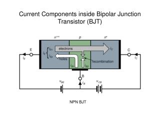
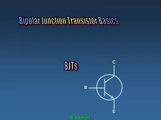
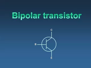
Draw like Streetman & Banerjee: • Emitter (p+) injects holes into reverse-biased Base-Collector. • For Collector to… collect all (most) holes we need Base to be quite_________. Mathematically, Wb << ______. • Properly biased, with BJT “on” the voltages are: VEB > ____ and VCB < ____ (same as VBC > ____). • If so, then almost all injected holes are collected: IE ≈ IC are the “large” currents here (water passing through the hose).
Is there a Base current IB? What does it consist of? • Base current IB (remember base is n-type for pnp BJT): • Some electrons____________ with injected holes. • Some electrons injected into p+ (forward biased EB). • Few electrons from thermal generation in reverse-biased CB junction • Base current IB is small, but it’s there. See figure for signs.
In a well-designed BJT, IE ≈ IC ≈ 100IB • We can write from current continuity: ______________ • There are both PNP and NPN bipolar transistors. • Easier to study PNP because current flows in direction of holes. But NPN is similar, replace holes w/ electrons and keep track of signs! • Intuitively (dimensions, doping being equal), which is faster?
BJT performance parameters: • Emitter efficiency: • Base transport factor: • Current transfer ratio: • Current amplification (common emitter gain):
Let’s begin to understand BJT physics. Think of it as two independent PN junctions: • Band diagram in equilibrium (all I=0): • Electric field: • Charge density:
ECE 340 Lecture 39Narrow-Base BJT • What did we learn so far? What is special about the Base? • Try to make things simple(r): • E B current is all holes (p+ to n) • Holes diffuse across base, ignore drift (how come?) • Ignore any small reverse current at CB junction • Ignore recombination (for now)
Reality check. This is what a more realistic BJT looks like: • What kind of BJT? • What is the cross-sectional area? • What’s with all the extra n+ and p+ regions? • What’s with all the SiO2?
Back to our simplified analysis of the P+NP (VEB>0, VCB<0): • We know all action is minority carrier diffusion, focus there: • In fact, all action is hole diffusion in base, get Δp there: • Where pn = ni2/NB
Now we can almost calculate collector (hole) current… • … because I get a nice (linear) slope from knowing WB << Lp • This is a narrow-base BJT, and we want it that way! Then: • Remember, only holes are “captured” by the Collector. Why?
To get Emitter current, don’t forget there is a small electron injection component from the n-type Base. • Draw these injected (minority) electrons in Emitter: • And remember the expression from long-base diode: • We can finally write the entire Emitter current:
Now we can calculate a lot of those “merit” parameters listed in the last lecture, like Emitter efficiency, • Finally, what is the Base current? • The current gain is
Expression for gain β can be simplified two ways: • 1) If there is no recombination in the Base, and IB is due only to electron injection back into Emitter: • 2) If Emitter efficiency is perfect (γ = 1) and IB is due only to recombination in the Base: • Where Lp = (Dpτp)1/2 is hole diffusion length in the Base, and by construction WB << Lp. • If you are not given Dp how do you calculate it?
Clearly (by construction) β >> 1 so we get CURRENT GAIN! • Why? (qualitatively). Draw energy band diagram, think about what happens if I pull a small current from Base (inject electrons).
ECE 340 Lecture 40BJT Normal Mode and Gain • Two main pictures for P+NP bipolar transistors:
Recap our simple model for P+NP bipolar operation: • Current continuity: IE = IB + IC • When EB diode is forward biased (VEB > 0), Emitter current IE has two components: • Holes it injects into the Base (IEp) • Electrons the n-type Base injects into it (IEn) • Base current has two components: • Electrons it draws from terminal to supply IEn • Electrons it draws from terminal to recombine with injected holes (QB/τp) • Collector current is made up of holes it manages to sweep (“collect”) from the ones injected by Emitter, minus those that have recombined in the Base, strictly speaking IC = IEp – QB/τp • Is Collector current made up of any electrons? • Does our current continuity assumption hold? • When and what can we ignore to simplify our life?
One more look at the equations for P+NP: • Where, remember Lp = (Dpτp)1/2 for holes in the Base. • How do we keep things straight? • Tip #1: Remember who is injecting what where (if it’s into the Base, then use Base parameters like Dp, Lp WB and NB) • Tip #2: If the terminal is “narrow” use its width instead of the minority carrier diffusion length there • Tip #3: QB,stored is just the area under the stored charge triangle in the Base (1/2 * height * width…) • Tip #4: On notation, if it’s unambiguous we don’t need the extra E/B/C super/subscript (Base is the only n-type chunk here, so Dp must be for… minority holes in the Base!) • Tip #5: Remember the (ex - 1) factor is what multiplies the equilibrium minority carrier concentration (e.g. ni2/NB)
So, why do I have GAIN?! (IC/IB ~ 100) • Ex: P+NP bipolar with NE=1018 cm-3 and NB=1017 cm-3. The quasi-neutral region width in the emitter is 1 μm and 0.2 μm in the base. Use μn=1000 cm2/Vs and μp=300 cm2/Vs. The minority carrier lifetimes are 10 ns. Calculate the emitter efficiency, the base transport factor, and the current gain of this transistor biased in the forward active mode. Assume there is no recombination in the depletion regions. (Note: are the emitter and base “narrow” or “wide”?)