Download
1 / 1

E N D
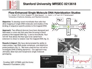
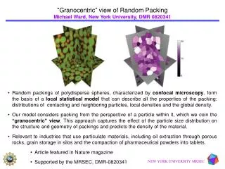
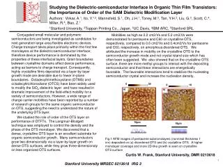
Conjugated small molecular and polymeric semiconductors are being investigated as candidates for next generation large-area flexible electronic devices. Charge transport takes place primarily within the first few monolayers at the dielectric/semiconductor interface; therefore device performance is dominated by the properties of these interfacial layers. Grain boundaries between crystalline domains affect device performance, acting as barriers to charge transport. Consequently, highly crystalline films deposited via a layer-by-layer growth mode are desirable due to fewer in-plane boundaries. Octadecyltrimethoxysilane (OTMS) and octadecyltrichlorosilane (OTCS) have been widely used to modify the SiO2 dielectric layer and have resulted in dramatic improvement of the field-effect mobility for a variety of semiconductors. However, a wide range of charge-carrier mobilities have been reported by a number of research groups for the same organic semiconductor on OTS, suggesting the need to understand the nature of the underlying OTS layer. We studied the role of order of the OTS layer on performance of OTFTs. The Langmuir-Blodgett technique was employed to control the density and the phase of the OTS monolayer. We discovered that a dense, crystalline OTS layer is an excellent substrate for organic semiconductor growth. Many semiconductors grow two-dimensionally via a layer-by-layer growth on dense OTS surfaces, while they grow three-dimensionaly on less organized OTS surfaces. Studying the Dielectric-semiconductor Interface in Organic Thin Film Transistors: the Importance of Order of the SAM Dielectric Modification Layer Authors: Virkar, A.1, Ito, Y.1.2, Mannsfeld, S.1, Oh, J.H.1, Toney, M.5, Tan, Y.H.3, Liu, G.3, Scott, C.4, Miller, R.4, Bao, Z.1 1Stanford University, 2Toppan Printing Co., Japan, 3UC Davis, 4IBM ARC, 5Stanford SRL Mobilities as high as 2.2 cm2/Vs and 5.2 cm2/Vs were demonstrated for pentacene and C60 on crystalline OTS, respectively, compared to 0.6 cm2/Vs and 0.4cm2/Vs for pentacene and C60, respectively, on amorphous disordered OTS. We attributed the increase in mobility on the crystalline OTS to the semiconductor growth mode and not crystal island size which has often been suggested. We also showed that on the crystalline OTS surface, there are more methyl groups to interact with the depositing semiconductor and that these interactions are energetically favorable. The favorable interactions tend to stabilize the nucleating semiconductor crystal and increase the nucleation density. a Fig.1 AFM images of pentacene submonolayers (norminal thickness 1 nm) deposited on (a) disordered OTS and (b) crystalline OTS. A higher monolayer coverage and more 2D-like growth is seen on crystalline OTS surface 10 μm Curtis W. Frank, Stanford University, DMR 0213618 1 Stanford University MRSEC 0213618 IRG 3