Efficient Load Balancing Switch for Multiprocessor Systems
Explore a system for parallel processing with high throughput, configurable hardware, and efficient resource utilization. Maximize data stream handling and achieve optimal system performance in a multi-FPGA environment. Learn about the Load Balancing Switch that improves workload distribution, monitors system loads, and ensures expandable design. Develop a smart management system converting shared resources to personalized workspaces. Efficiently manage multiple parallel units and enhance system scalability. Dive into the hardware and software components, clusters configuration, and the system's input/output interfaces for seamless data processing. The project aims to tackle challenges in data stream management, parallel unit utilization, and resource efficiency, offering innovative solutions for improved performance.


Efficient Load Balancing Switch for Multiprocessor Systems
E N D
Presentation Transcript
Midterm presentation for project By: Oleg Schtofenmaher Maxim Fudim Supervisor: Walter Isaschar • Winter 2007 ( Part A) LOAD BALANCING SWITCH
General overview • Software solutions for real-time are too slow • Power dissipation limits work frequencies • Greater computing power needed • H/W accelerators can improve S/W processes • Multi-core, multi-threaded systems are the future
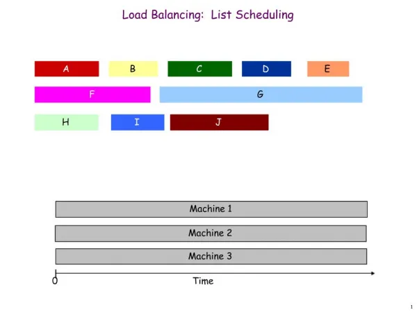
Project Goals • Multiprocessor environment for parallel processing of vectors data stream • Maximal Throughput • Configurable hardware • Statistics report • Expandable design
System specifications • 1M pulse/sec data stream • Vectors of 8 ÷ 1024 pulses • 1K ÷ 125K vectors/sec • Variable number of accelerators • Timeout of 100msec • System span over multiple FPGAs
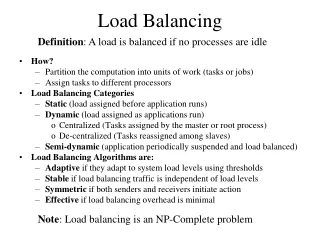
Problem • How to manage Data stream? • How to manage multiple parallel units? • How to achieve full and effective utilization of resources?
Solution • Load Balancing Switch • Converting shared resources to “personal” work space. • Smart management of system • Monitoring of each unit’s load • Easily expandable
System Block diagram S/W or H/W generator DDR2 Bank A Input vectors Load Balancing Switch (LBS) NIOS VPU NIOS VPU S/W or H/W consumer Data and Control DDR2 Bank B Output reports PROCStar II Stratix II FPGA
Organization of VPU’s(Vector Processing Units) • NIOS VPUs joined into the clusters • Constant number of Clusters • Various number of NIOS VPU’s in cluster • Variable configuration of NIOS • Different Priority for different clusters
System Top Diagram NIOScluster NIOScluster NIOScluster NIOScluster DDR2 Bank A Input vectors NIOScluster NIOScluster NIOScluster NIOScluster Load Balancing Switch (LBS) Gidel’s FIFO control IP Data flow NIOScluster NIOScluster NIOScluster NIOScluster DDR2 Bank B Output reports NIOScluster NIOScluster NIOScluster NIOScluster Stratix II FPGA PROCStar II
LBS Top Level View FIFO Input Port Input data bus Cluster Arbiter Cluster Arbiter Cluster Arbiter PCI Input Reader NIOS II System NIOS II System NIOS II System Control Main Controller unit Statistics Reporter Control Control and Status Output Writer Control FIFOOutputPort Muxed output data bus Stratix II FPGA
System Interfaces Software to Hardware Interface: • Input and Output MultiFIFO PCI data bus • MultiFIFO status flags • 2x32-bit general read purpose registers • 2x32-bit general write purpose registers • 8-bit information register • Software reset signal
Input System Interface LBS Input Interface: • 64 bit data bus from Input MultiFIFO • Read request and ack. Signals • MultiFIFO status flags • SW/HW input signals
Output System Interface LBS Output interface: • 64 bit data bus to Output MultiFIFO • Write request and ack. Signals • MultiFIFO status flags • SW/HW input signals
Data Packet Format …… Header Tail Data 1 to N Words Header : SW/HW Control 1-bit Unused Nios Number Data Length Vector ID Type 1-bit Version 4-bit 8-bit 16-bit 32-bit Tail : Sync Data or Checksum(in the future)
NIOS Input Interface Hardware: • 64-bit input data bus – from LBS • 10 bit data slices counter – from LBS • Write request signal – from LBS • Chip select signal – from LBS • NIOS ready signal – from NIOS • Data ready signal – from LBS
NIOS Output Interface Hardware: • 64 bit output data bus – from NIOS • 7 bit data slices counter – from LBS • Read request signal – from LBS • Chip select signal – from LBS • Output ready signal – from NIOS • Output taken signal – from LBS
FIFO Input Port Input data bus LBS Units DescriptionInput Reader Input Reader Main Controller unit Statistics Reporter Control and Status Output Writer FIFOOutputPort Muxed output data bus • Reading data from input FIFO • Writing data to selected cluster • Providing header control bits for main controller • Synchronization checks • Vector length counter Cluster Arbiter Cluster Arbiter Cluster Arbiter NIOS II System NIOS II System NIOS II System
FIFO Input Port Input data bus LBS Units DescriptionOutput Writer Input Reader Main Controller unit Statistics Reporter Control and Status Output Writer FIFOOutputPort Muxed output data bus • Reading data from selected cluster • Writing data to output FIFO • Vector length counter Cluster Arbiter Cluster Arbiter Cluster Arbiter NIOS II System NIOS II System NIOS II System
FIFO Input Port Input data bus LBS Units DescriptionMain Controller Input Reader Main Controller unit Statistics Reporter Control and Status Output Writer FIFOOutputPort Muxed output data bus • Enabling input and output units • Selecting control source (S/W or H/W) • Monitoring clusters’ load via status buses • Selecting clusters for input/output operations • Data validity indication Cluster Arbiter Cluster Arbiter Cluster Arbiter NIOS II System NIOS II System NIOS II System
LBS Units DescriptionMC Status Alghoritm • Status input and output independent decoders • Dynamic port mapping • Always selecting closest active neighbor • Suits “similar NIOSes” design • To be expanded in part B
FIFO Input Port Input data bus LBS Units DescriptionStatistics Reporter Input Reader Main Controller unit Statistics Reporter Control and Status Output Writer FIFOOutputPort Muxed output data bus • Monitoring system activity • Counting processed vectors • Throughput = Vectors served / Time of service • To be expanded in part B Cluster Arbiter Cluster Arbiter Cluster Arbiter NIOS II System NIOS II System NIOS II System
FIFO Input Port Input data bus LBS Units DescriptionCluster Entity Input Reader Main Controller unit Statistics Reporter Control and Status Output Writer FIFOOutputPort Muxed output data bus • Cluster parametric enabling • Cluster controller • Watchdog • NIOS System Cluster Arbiter Cluster Arbiter Cluster Arbiter NIOS II System NIOS II System NIOS II System
LBS Units DescriptionCluster Controller • Input 4-phase REQ/ACK protocol with NIOS • Nios Ready • Data Ready • Output 4-phase REQ/ACK protocol with NIOS • Output Ready • Output Taken • Smart Status Reporter
LBS Units DescriptionExample for NIOS System • SOPC components: • Input Vector • Output Vector • Nios II • On-chip memory • Timer
LBS Units DescriptionInput vector • Export signals from LBS • 64-bit data • Nios/Data Ready • Address , Chipselect , Write request ,Clock , Reset • On-chip memory for 1024 32-bit words • Avalon slave data port for 32-bit data to NIOS II • Avalon slave data ready port
LBS Units DescriptionOutput vector • Avalon slave 32-bit data output port from NIOS II • Avalon slave output ready port • On-chip memory for 128 32-bit words • Export signals to LBS • 64-bit data • Output Ready / Taken • Address , Chipselect , Read request ,Clock , Reset
Tasks • Study PROCStar Board – Done • Study Altera’s Stratix II FPGA – Done • Study Quartus and HDL designer– Done • Study GIDEL API – Done • Learn to use Signal Tap tool – Done • Study Altera’s NIOS II – Done • Define interface with software group –Done • Develop signal generator for testing – Done
Tasks (cont.) • Define interface with accelerator group – Done • Build direct connection with s/w and NIOS II – Done • Expand design for several NIOS’s – Done • Define basic algorithm for h/w switching – Done • Implementation and debugging of the switch – Done • Integration of entire system – Done • Create Test application for operating with hardware design – Done
Tasks for Part B • Increase number of Nios’s in clusters • Spread design to several FPGAs • Improve algorithm for cluster selection • Expand statistic reports • Expand SW/HW communication • Add error correction/handling