Download
1 / 101
1.01k likes | 1.21k Views
Explore various compensation designs for control systems using root locus analysis with practical examples and step responses.

E N D
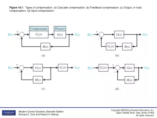
Figure 10.1 Types of compensation. (a) Cascade compensation. (b) Feedback compensation. (c) Output, or load,compensation. (d) Input compensation.
Figure 10.5 Maximum phase angle Φmversus α for a phase-lead network.
Figure 10.10 (a) Bode diagram for Example 10.2. (b) Nichols diagram for Example 10.2.
Figure 10.11 Compensation on the s-plane using a phase-lead network.
Figure 10.13 (a) Design of a phase-lead network on the s-plane for Example 10.4. (b) Step response of the compensated system of Example 10.4.
Figure 10.15 The s-plane design of an integration compensator.
Figure 10.16 Root locus of the uncompensated system of Example 10.6.
Figure 10.17 Root locus of the compensated system of Example 10.6. Note that the actual root will differ from the desired root by a slight amount. The vertical portion of the locus leaves the σaxis at σ = -0.95.
Figure 10.18 Design of a phase-lag compensator on the s-plane.
Figure 10.19 (a) Design of a phase-lag network on the Bode diagram for Example 10.8. (b) Time response to a step input for the uncompensated system (solid line) and the compensated system (dashed line) of Example 10.8.
Figure 10.20 Design of a phase-lag network on the Bode diagram for Example 10.9.
Figure 10.23 The deadbeat response. A is the magnitude of the step input.
Figure 10.24 (a) Rotor winder control system. (b) Block diagram.
Figure 10.26 (a) Step response and (b) ramp response for rotor winder system.
Figure 10.28 Root locus for the pen plotter, showing the roots with a damping ratio of . The dominant roots ares = -4.9 ± j4.9.
Figure 10.30 A simplified block diagram of the milling machine feedback system.
Figure 10.31 Elements of the control system design process emphasized in this milling machine control system design example.
Figure 10.32 Hypothetical impulse response of the milling machine.
Figure 10.35 (a) Transient response for simple gain controller. (b) m-file script.
Figure 10.36 (continued) (a) Bode diagram. (b) m-file script.
Figure 10.37 Lead compensator: (a) compensated Bode diagram, (b) m-file script.
Figure 10.38 Lead compensator: (a) step response, (b) m-file script.
Figure 10.39 Lag compensator: (a) uncompensated root locus, (b) m-file script.
Figure 10.40 Lag compensator: (a) compensated root locus, (b) m-file script.
Figure 10.41 Lag compensator: (a) step response, (b) m-file response.
Figure 10.42 Disk drive control system with PD controller (second-order model).