Download
1 / 16
160 likes | 303 Views
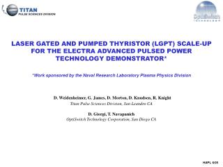
LASER GATED AND PUMPED THYRISTOR (LGPT) SCALE-UP FOR THE ELECTRA ADVANCED PULSED POWER TECHNOLOGY DEMONSTRATOR* *Work sponsored by the Naval Research Laboratory Plasma Physics Division D. Weidenheimer, G. James, D. Morton, D. Knudsen, R. Knight Titan Pulse Sciences Division, San Leandro CA

E N D
LASER GATED AND PUMPED THYRISTOR (LGPT) SCALE-UP FOR THE ELECTRA ADVANCED PULSED POWER TECHNOLOGY DEMONSTRATOR* *Work sponsored by the Naval Research Laboratory Plasma Physics Division D. Weidenheimer, G. James, D. Morton, D. Knudsen, R. Knight Titan Pulse Sciences Division, San Leandro CA D. Giorgi, T. Navapanich OptiSwitch Technology Corporation, San Diego CA
LGPT Concept CONCEPT LGPT (Laser Gated & Pumped Thyristor), • Flood entire switch channel with laser light… • Optical fluence determines di/dt • Advances in design, construction yield fast thyristor action (» 100 ns) • Near band edge light, high quality silicon enable 20 kV working devices • Continuous illumination reduces forward dissipation in thyristor • Uses relatively low power laser diodes in place of YAG n++ p Diode Lasers On or off-board n- n+ p++ Si Switch
Development History I Limited Area Developmental Devices
Development History II No. of shots to failure vs. current density at 162-184 kA/usec/cm2
Development History III No. of shots to failure vs. di/dt density at 15 kA/cm2 current density
Development History IV Laser Diode Bars Circa 2000-2003 – first designs - standard cavity, 1085 thru 1125 nm progression in wavelength, 60 x 1500 um x 90 um pitch, 2500 um bar length, stripline package 2004 - first LOC strain-mitigated designs - reduced facet loading, 1125 nm, increased emitter area/packing fraction, 150 x 2000 um x 180 um pitch, 2500 um bar length, increased lifetimes at requisite drive currents 2005 - first LOC designs with single-side confinement, 1125 nm, further reduced facet loading – longer life expectations, 140 x 2000 um x 170 um pitch, same bar length, due 6/05 first direct-coupled double-layer mini-bars, 2 emitter arrays ~150 um c-c, same package envelope, due 7/05
Development History V Laser Diode Bars Apparent turn-on delay (fill-time) of diode laser cavities – reproducible for fixed drive parameters
Development History VI Laser Diode Bars Thermal CWL Shift and Spectral Broadening with Current
Development History VII Silicon Thyristors • Basic design has remained unchanged since late • 2002 – quasi-symmetric thyristor, 16.4 kV working • Continuous iterations/improvements made to • passivation and encapsulation, optical interface, • current contacts • Co-planar anti-parallel diodes added 2004
Floating Laser Power/Trigger Circuit Load ( Twelve 55W Rs) Three Tek HV probes for Charge, Load R, and LGPT R Circuit L LGPT V Monitor B-dot Circuit C Development History VIII Diagnostics/Test Fixtures • Improved diagnostics • measure forward voltage drop • with confidence – forward • dissipation • SF6 device immersion enables • rapid turn-around between • failures, maintenance and • inspections
Recent Conclusions • Experimental measurements/data, Medici modeling, absorption profiles, • ray-tracing, plasma-spread theory all point to active silicon volume being • confined to that defined by the window/cell dimensions. • Devices must be scaled by the cell unit – presently ~.0167 cm2 • Current density of ~15 kA/cm2 and di/dt density of ~90 kA/usec/cm2, • corresponding to illumination levels of ~25 kW/cm2 (gross-active)are • sustainable for ~107 shots at 5 pps by both silicon device and latest design • lasers – 800 nsec half-sine pulseshape • Reduction in current and di/dt density by a factor of 2, with commensurate • reduction in optical illumination levels should be sufficient for ~109 shot • service at 5 pps • Scaled-up integrated device design must have flexibility to accommodate a range • of 7-15 kA/cm2 active area and the requisite laser diode bars to provide • illumination levels from ~12-25 kW/cm2 (active) in a device with an overall • peak current rating of 10-20 kA, di/dt of 60-200 kA/usec • Cell/laser bar counts for such a device will be from 40-80 at present cell • dimensions – fewer if cell/laser bar size increases • Scale-up requires direct-mount double bar laser packaging and series drive
LGPT Scale-Up 5 x 1 cm LGPT LGPT Integrated with Electrodes/Lasers • ~ 5 cm x 1 cm contact area device accommodates 42 cells in first iteration • Staggered patterning of cells for greater active area packing fraction • Expandable to 84 cells as necessary • Single laser diode bar each cell in first iteration – 5-10 kA peak current - 7/05 • Direct-coupled double laser package upgrade - >10 kA peak - 8/05 • Expansion to 84 cells – if necessary – 9/05
Scaled-Up Test Capability • Integrated LGPT inserts into scaled- • up test fixture • Fast turn-around features • Peak currents to >25 kA • Full diagnostics as in small scale testbed • Easy access to all internal components • Components to undergo miniaturization • phase after scaling demonstrated
Summary/Conclusions • Understanding of LGPT performance/scaling is sufficient to move ahead with 5 x 1 cm • KrF IFE building-block device • Scaled-up device and test fixture designs completed ~April, 2005 • Silicon devices are in process at Optiswitch, due for first delivery by end of June, 2005 • Electrodes/laser drive hardware for 1st prototype due end of June • First single bar packaged limited confinement LOC laser bars due end of June • Direct double bar packaged lasers due in July, 2005 • Subsystem testing to begin early July • Full integrated device testing in late July • Engineering iterations/optimizations through 2005-2006 • Target retro-fit of FE2 in 2006-2007