Download
1 / 8
80 likes | 235 Views
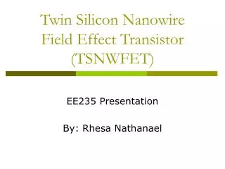
Nanowire Size Dependency on TSNWFET. Ref.: S. D. Suk et al ., “Investigation of nanowire size dependency on TSNWFET”, IEDM Tech. Dig ., pp. 891-894, 2007. Xin Sun April 16, 2008. Introduction. Gate-all-around nanowire MOSFET. d NW splits from 0nm to 11nm. High performance

E N D
Nanowire Size Dependency on TSNWFET Ref.: S. D. Suk et al., “Investigation of nanowire size dependency on TSNWFET”, IEDM Tech. Dig., pp. 891-894, 2007. Xin Sun April 16, 2008
Introduction Gate-all-around nanowire MOSFET dNW splits from 0nm to 11nm • High performance • Ideal gate controllability
ID-VG Characteristics • As dNW decreases, • VTH increases due to conduction band increase in limited dimension of nanowire channel. • ION decrease
Current Drivability Surface and phonon scattering increase
Short Channel Control • Minority carriers can be easily trapped to gate oxide by larger vertical electric field on surface. • Influence of surface conditions to channel can be enhanced with smaller nanowire.
Capacitance 100x100 arrays Volume inversion
Mobility Right part: volume inversion effect exceeds scattering effect. Left part: scatterings are dominant.
Conclusion • Volume inversion is first confirmed by capacitance measurement on TSNWFET with various channel size. • 4nm is the optimal channel size.