Download
1 / 22
220 likes | 237 Views
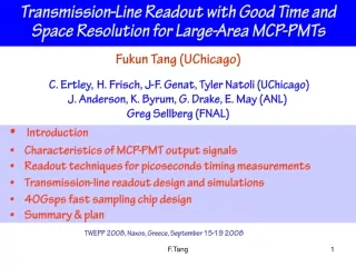
Transmission-Line Readout with Good Time and Space Resolution for Large-Area MCP-PMTs. Fukun Tang (UChicago)

E N D
Transmission-Line Readout with Good Time and Space Resolution for Large-Area MCP-PMTs Fukun Tang (UChicago) C. Ertley, H. Frisch, J-F. Genat, Tyler Natoli (UChicago) J. Anderson, K. Byrum, G. Drake, E. May (ANL) Greg Sellberg (FNAL) • Introduction • Characteristics of MCP-PMT output signals • Readout techniques for picoseconds timing measurements • Transmission-line readout design and simulations • 40Gsps fast sampling chip design • Summary & plan TWEPP 2008, Naxos, Greece, September 15-19 2008 F.Tang
Introduction: Applications of Time-of-Flight for HEP Courtesy of H. Frisch Collider Detector (H. Nicholson) F.Tang
Introduction: Planacon MCP-PMT Tube & Anode Array Charged Particle Photon Photoelectric cathode Electron pores with gain of 105-106 Pore Size 25u 1024 anode pads (1.1x1.1mm), with pitch of 1.6mm Electron Shower To Electronics F.Tang
MCP signals Courtesy of J-F. Genat SLAC Jerry Va’Vra 400ps • Measured (beam-tests) : Simulation: • Rise-time: 380ps - Rise time 200ps (6mm pores) bw=1.75GHz • - 25mm pores - Time spread: +/- 125ps, random • - Amplitude spread: 14%, normal F.Tang
MCP signals (beam-test) • Use many fewer readout electronics channels • Use many fewer readout electronics channels 25 mm pores Two stages MCP Gain ~106 As measured at Fermilab (beam-test, 10-50 PEs) SLAC Jerry Va’Vra 400ps I (1PE) = dQ/dt ~1.6x10-19 x 5 x105/ 250 ps = 320 uA Expect: 16 mV @ 50 W F.Tang
Fast Timing Electronics Current techniques: • Leading edge + TDC/ADC • Constant fraction + TDC/ADC • Zero-crossing + TDC • Double / multiple thresholds + TDC/ADC • Pulse sampling and reconstruction The most favorable method is sampling, particularly in the case of few Photo-electrons. Samples as effective for timing as steep signal slope and large signal/noise ratio Use today existing sampling chips in first step: Hawaii, PSI, Saclay/Orsay (sampling rate @2-5 GHz, 10-13 bits) - Derive accurate time and charge using digital signal processing - Resolve pile-up, transmission line readout ambiguities F.Tang
Monte-Carlo simulations • MCP signals • - 200ps rise time • 400ps fall time • 10-100 Photo-electrons • MCP noise 50% • White noise 50% • S/N 10-100 • Fast Sampling simulation • - Sampling frequency 40 Gsps Fast timing simulations • Pulse sampling • Assume 1.5 GHz analog bandwidth: • 100 samples taken at 10-40 Gsps allow reconstructing time to a few picoseconds and charge to one per cent. • Better time resolution compared to CFD particularly at low PEs, • Records the full pulse information F.Tang
Proposed Transmission –line and Fast Sampling Readout for Planacon MCP-PMT Why use transmission-line readout? Advantages of transmission-line and fast sampling techniques: • Use many fewer readout channels (1024 down to 64 channels) • Readout timing, position and energy information • Good transmission-line bandwidth (up to 3.5GHz ) F.Tang
Principle of Transmission-line Anode Readout t0 t1 t2 40Gsps Pulse Sampling 40Gsps Pulse Sampling sampler sampler sampler Timing: ( Sampling over the peak) Position: Energy: (Full waveform sampling) F.Tang
2’ Ch0R Ch0L Proposed Transmission-line Anode Board (top view) 32 vias each side 2’ 32 microstrip Z=50W lines Width=1.1mm Pitch=1.6mm Ch31L Ch31R F.Tang
Prototype Transmission-line Readout Board Design and Simulations Based on Commercial 2’x2’ 1024-Anode Tube Interconnection: (1) Elastomer (2) Low-T solder (indium) (3) Conductive Epoxy (4) Ultimately capacitive coupling Transmission Line Readout Board F.Tang
Layout of Prototype Transmission-line Readout Board Trace length: 5.36’, 4.83’ , 3.97’ Board Size: 130x60mm Board Thickness: 1.2mm Tube Outline 58x58mm F.Tang
t = 9.7ps < 0.5tr cL cL Bandwidth Analysis for Transmission-line Readout Simplified model with the transmission-line readout board attached to MCP-PMT: Zo’ <= 50 Z0=50 Z0=50 2-inch Line 32 Pad Stubs Equal distributed 32 CL=100falong 2-inch line, It reduces impedance to Zo’, However, it also reduced the BW. F.Tang
System Modeling for Transmission-line Readout Simulation HV2 Pores HV1 Ca32 Impedance discontinuity caused by vias and ball contacts Ca1 Transmission-Line Anodes (Z0’) 2-inch Via size: 15x10x5 mils Board Thickness: h=62mils 1 inch 1 inch Lv=0.3n, Cv=150f Pulse Sampling Z0=50 Z0=50 Zvia=31.6W 40GspsSampling Chip 40Gsps Sampling Chip Lv 2-in Line Anodes Lv Z0 Z0 Z0’ Cv2 Cv Cv F.Tang
Outputs on Each End of Transmission-line with Stub Anodes (hit at pad-5) Electrons Input Force: Tr=tf=200ps Out_R Out_L 32 1 5 Output on left_end (t1) Reflection caused by impedance mismatch and discontinuity Output on right_end (t2) F.Tang
Outputs on Each End of Transmission-line with Stub Anodes (hit at pad-16) Responses with Hit on Pad-16 Input on Pad-16 Out_L Out_R Electrons Out_R Out_L 32 1 16 tr=tf=100ps Baseline settled after a few ns F.Tang
Outputs on Each End of Transmission-line without Stub Anodes (hit at the same position as pad-16) Electrons Input force Out_L Out_R Out_R Out_L 32 1 16 F.Tang
Simulation with Transmission-Line Anode up to 48-inches Simulation Goal: To understand analog signal bandwidth vs. the length of transmission-line for MCP anode design. System Setup: The simulation model is extracted from a board layout. The transmission-line impedance Z=50 ohms, the length is 48-inch with 4824 tapped anodes which induce 100f capacitance each. Input Force: A step voltage input force with a rise time of 100ps, an amplitude of 1.4Vexcites the line at the point 1-inch from the left end. Outputs: Comparing the rise time between both ends of the line. 4824 anodes Tr=100ps Step Voltage Source OUT_L1in OUT_R47in a1 a2 a4824 a5 50 50 Simulation Setup F.Tang
Responses on each end of 48-inch transmission-line (Hit at the position 1-ch to the left) Input Force Tr=100ps Output on Right (47-inch to the source) Output on Left (1-inch to the source) Tr=319ps measured by simulation tool. Corresponding to analog bandwidth of 1.15GHz F.Tang
ch0L ch0R Conceptual Design of Transmission-line and Fast Sampling Readout Electronics 64-CH 40Gsps Analog Sampling Chips Only 64-ch readout electronics needed! FPGA Cable Conn ch31L ch31R F.Tang
Technology: IBM 8RF DM 130nm CMOS design kit from CERN • Key numbers of UChicago Fast Sampling Chip • -- 40 GHz sampling • -- 1-2 GHz analog bandwidth • -- 8 -10 bit ADCs • -- Self/Global trigger • -- Time Stamping • -- Readout protocols • Work in Progress: • Unity gain input buffer design(1-2GHz BW) • Analog bandwidth is 1.6 GHz (-3dB) using current mode amplifier has been achieved (pre-layout). • To be improved: • Tuning input impedance of 200W to 50 Wwith • the IBM130nm CMOS DM (analog RF) process when available. • --Extend analog bandwidth as far as possible, if input buffer can not meet the requirement. • Sampling timing generator design • Sampling cells and ADCs: Experience from Orsay/Saclay, Hawaii and PSI. • Expect 2-3ps timing resolution with MCP signals Fast sampling chip at UChicago F.Tang
Summary Advantages: • Use many fewer readout electronics channels • Readout timing, position and energy information • Good signal bandwidth • Easy to match impedance all the way to the chip input • Plans (short and long term) • Prototyping transmission-line readout with laser stand and 40Gsps scope (in few weeks) • Transmission-line readout with two LAB2 or two DRS4 Chips (possibly 2x interleaving?) (in few months) • Development of 40Gsps sampling chip for large scale detectors • ---2-ch demonstration chip with IBM 8RF 0.13u CMOS (year 1) • --- 32/64-ch chip (year 2) • Built-in transmission-line anode design and simulation (need to work with tube designers) F.Tang