Download
1 / 21
210 likes | 227 Views
Discover how MEMS (Micro Electro Mechanical Systems) impact our daily lives through sensors and actuators. MEMS are key components in airbag sensors, accelerometers, inkjet printers, and HDTV sets. Learn about lithography, the process of creating MEMS using precision techniques, and how microdevices are fabricated to enhance technology. This educational guide introduces you to the world of MEMS and their application in various industries. For more information, contact joecho@mail.ucf.edu.

E N D
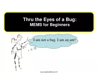
Thru the Eyes of a Bug: MEMS for Beginners I am not a bug. I am an ant! NanoFab&BioMEMS @ UCF
MEMS? I guess you might never heard of MEMS.. NanoFab&BioMEMS @ UCF
Where? Tell me. MEMS stands for Micro Electro Mechanical Systems and we have a plenty of them in our daily lives… Me? Super Ant NanoFab&BioMEMS @ UCF
In cars, the airbag sensor is one.. This saved my life! Airbag From www.lanl.gov/quarterly/q_sum03/airbags.shtml NanoFab&BioMEMS @ UCF
Inside of the airbag sensor, a key component is an accelerometer, which detects a sudden motion and send an electrical signal to deploy the airbag. Got it? A mechanical motion and an electrical signal are bridged. MEMS Micro Electro Mechanical Systems NanoFab&BioMEMS @ UCF
Let’s talk about “micro”, then. This is a photo of the accelerometer. Source: Analog Devices Inc. Human hair NanoFab&BioMEMS @ UCF
I am bigger than MEMS! MEMS MEMS The diameter of a human hair is about 50 t0 100 micrometers. 1,000 micrometers become 1 milimeter. Anything smaller than micro? It’s nano. 1,000 nano = 1 micron NanoFab&BioMEMS @ UCF
Source: Texas Instrument, http://www.dlp.com/ This is an array of MEMS mirrors. Yes, the ant is much bigger.. NanoFab&BioMEMS @ UCF
Cool~! Let’s take a close look. These moving mirrors are used for HDTV sets and projectors. Source: http://www.dlp.com/ NanoFab&BioMEMS @ UCF
http://www.interconnect-solutions.com/inkjet-printing.html Hole for ink droplet http://mimech.com/printers/inkjet-printer-technology.asp http://konicaminolta.com/ We can also find a MEMS component in an inkjet printer. NanoFab&BioMEMS @ UCF
As we can see, most of MEMS components are either used for measuring and detecting real world conditions (sensors) or for generating a motion (actuators). Sweet~ Sensor Actuator NanoFab&BioMEMS @ UCF
What is lithography? In summary, miniaturized sensors, actuators and systems fabricated by the use of lithography and/or other precision techniques are called MEMS. NanoFab&BioMEMS @ UCF
I will explain… Need to wear my glasses. NanoFab&BioMEMS @ UCF
Litho means “stone” Graphy means “writing” Original designs are drawn on a hard surface (like a limestone) and they are transferred to a soft substrate (like a paper). NanoFab&BioMEMS @ UCF
The traditional lithography technique uses ink for the pattern transfer. In MEMS technology, a “mask”, “light” and a “photoresist” are used. A mask is similar to a film in a camera. The original design on a mask is transferred to a photoresist. The photoresist is sensitive to light and changes its chemical structure upon exposure. NanoFab&BioMEMS @ UCF
Instead of paper, we use a silicon wafer and coat it with a photoresist, then expose it under the mask. Using lenses we can reduce the size of the image easily. Yes, down to the micron level. NanoFab&BioMEMS @ UCF
The exposed photoresist can be dissolved(+) or left behind(-) after a chemical treatment. Negative Photoresist Mask PositivePhotoresist This process is called development. Light NanoFab&BioMEMS @ UCF
Source: IEEE Spectrum See how it works? NanoFab&BioMEMS @ UCF
Step 1 Step 2 Step 3 Step 4 Eureka! Repeating this photolithography process with deposition and/or etching, we can create complex multilayered structures like this NanoFab&BioMEMS @ UCF
Do you know what this is? If so, please send an email to joecho@mail,ucf.edu Welcome to the world of MEMS! Source: NanoFab and BioMEMS Lab @ UCF Silicon Sensing Systems Ltd., Lucas NovaSensor, Sandia National Lab NanoFab&BioMEMS @ UCF
Produced by Prof. H. J. Cho • “Ant” character created by A. Wesser • Under the support of National Scicence Foundation • NSF CAREER ECS 0348603 • Coming up… soon. • Thru the eyes of a Bug • BioMEMS for beginners • If you need a copy of this for educational purpose, • please contact joecho@mail.ucf.edu with your name and school name. NanoFab&BioMEMS @ UCF
![Modeling MEMS Sensors [SUGAR: A Computer Aided Design Tool for MEMS ]](https://cdn2.slideserve.com/5124381/modeling-mems-sensors-sugar-a-computer-aided-design-tool-for-mems-dt.jpg)