Download
1 / 32
330 likes | 538 Views
Dual-V DD Pass Transistor Logic. Jeff Brantley and Sam Ridenour. Problem. Pass transistor logic (PTL) Pros Reduced area (when nMOS -only) Reduced leakage (fewer PUNs and PDNs) Cons “Weak 1” (V T drop) Increased delay / roll-up time “Sneak” leakage paths

E N D
Dual-VDD Pass Transistor Logic Jeff Brantley and Sam Ridenour
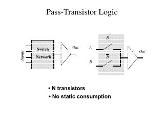
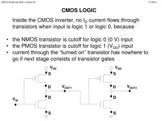
Problem • Pass transistor logic (PTL) • Pros • Reduced area (when nMOS-only) • Reduced leakage (fewer PUNs and PDNs) • Cons • “Weak 1” (VT drop) • Increased delay / roll-up time • “Sneak” leakage paths • Goal: improve delay & leakage without sacrificing pros
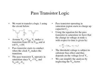
Approach • Use dual-VDD rails, with higher rail for gates • Eliminates VT drop through transistor becauseVG – VT >= VS • Decreases delay through nMOS channel • Explore relationship of E-D improvement to relative activity in select lines, input lines • Arrange select and input lines to reduce occurrence of sneak leakage • Specifically, re-order LUT input lines to achieve a corresponding LUT SRAM pattern that reduces leakage
Mux Structure S0Bar X0 S1Bar S0 X1 Out S0Bar S1 X2 S0 X3
Select0 (VDD + 300mv) Select0 (VDD) MuxOut (VDD + 300mv) MuxOut (VDD)
Case 1: LUT Inputs 4 16 Out SRAM Mux
Case 2: Mux Routing SRAM 4 16 Out Inputs Mux
Sneak Leakage S0Bar ‘1’ S1Bar S0 ‘0’ Out S0Bar S1 ‘1’ S0 ‘0’
Sneak Leakage Reduction • For a given LUT SRAM vector • For each possible permutation of select lines • Re-order the SRAM bits accordingly • For each value of the select lines • Count the 1T-off paths between every bit pair • Calculate probability of each select lines vector based on the P1 of each select line • Take the probability-weighted sum of all 1T-off counts • This value is the leakage score for that permutation • Choose the permutation with lowest score
Leakage Reduction • Overall leakage reduction stats: • (Over 30 random select line probability vectors)
Conclusions • Dual-VDD • Significant improvement in delay can be achieved for minimal energy cost for an nMOS PTL mux • Especially when select lines change infrequently relative to inputs • Thus, better results for routing than for LUT • Limitations (did not include in tests): • Cost of step-up / sense-amp between VDD regions • Actual SRAM bitcells • Large circuit (e.g. FPGA), area and power of extra VDD
Conclusions • Sneak leakage reduction • Initial results promising, but… • In context, the PTL sneak leakage is small relative to leakage in static circuits (SRAM bitcells, inverters, buffers)