Download
1 / 14
140 likes | 356 Views
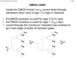
V DD. S. V OUT1. D. D. S. CMOS LOGIC. Inside the CMOS inverter, no I D current flows through transistors when input is logic 1 or logic 0, because the NMOS transistor is cutoff for logic 0 (0 V) input the PMOS transistor is cutoff for logic 1 (V DD ) input

E N D
VDD S VOUT1 D D S CMOS LOGIC • Inside the CMOS inverter, no ID current flows through transistors when input is logic 1 or logic 0, because • the NMOS transistor is cutoff for logic 0 (0 V) input • the PMOS transistor is cutoff for logic 1 (VDD) input • current through the “turned on” transistor has nowhere to go if next stage consists of transistor gates VDD S VOUT2 D D VIN S
ID(N) (= -ID(P)) X VOUT VDD VIN = 0 V VIN = VDD • NMOS transistor cutoff (since VGS(N) = VIN = 0 V) “acts as open circuit” • PMOS transistor “on” (VGS(P) = VIN – VDD = -VDD) but ID(P) = 0 A => VDS(P) = 0 V • PMOS transistor cutoff (VGS(P) = VIN – VDD = 0 V) “acts as open circuit” • NMOS transistor “on” (VGS(N) = VIN = VDD) but ID(N) = 0 A => VDS(N) = 0 V ID(N) (= -ID(P)) X VOUT VDD
D G S EASY MODEL FOR LOGIC ANALYSIS There is a simpler model for the behavior of transistors in a CMOS logic circuit, which applies when the input to the logic circuit is fully logic 0 or fully logic 1. VGS = VDD (for NMOS) VGS = -VDD (for PMOS) VGS = 0 V Each transistor will be in one of these two situations! D G S We can use the model to quickly determine the logical operation of a CMOS circuit (but we cannot use it to find circuit currents or voltages that will occur for mid-range input voltages).
REVISIT CMOS INVERTER WITH SIMPLE LOGIC MODEL Fill in the switch positions below… VDD VDD VOUT VIN = 0 V VOUT VIN = VDD
VDD CMOS NAND S S A PMOS1 PMOS2 F B NMOS1 S NMOS2 S
Verify the logical operation of the CMOS NAND circuit: VDD VDD S S S S A = 0V A = 0V F F B = 0V B = VDD S S S S
Verify the logical operation of the CMOS NAND circuit: VDD VDD S S S S A = VDD A = VDD F F B = 0V B = VDD S S S S
CMOS NOR VDD S A PMOS1 S B PMOS2 F NMOS1 NMOS2 S S
Verify the logical operation of the CMOS NOR circuit: VDD VDD S A = 0V S A = 0V S B = 0V S B = VDD F F S S S S
Verify the logical operation of the CMOS NOR circuit: VDD VDD S A = VDD S A = VDD S B = 0V S B = VDD F F S S S S
PULL-UP AND PULL-DOWN DEVICES In our logic circuits, the NMOS transistor sources are connected to ground, and the PMOS sources are connected to VDD. Notice that when NMOS transistors are “on” (when VGSN = VDD) VDSN is shorted by switch, helping connect output to ground. The NMOS transistor functions as a pull-down device; when active, it brings the output to 0 V. When PMOS transistors are “on” (when VGSP = -VDD) VDSP is shorted by switch, helping connect output to VDD. The PMOS transistor functions as a pull-up device; when active, it brings the output to VDD.
LIMITATIONS OF SWITCH MODEL In reality, the pull-up devices must have some VDS voltage and current flow to bring the output high since natural capacitance must be charged. Preview of next class: VDD S S A Similarly, the pull-down devices must have some VDS voltage and current flow to bring the output to ground since natural capacitance must be discharged. PMOS1 PMOS2 F B NMOS1 S NMOS2 S This is GATE DELAY.
LIMITATIONS OF SWITCH MODEL Suppose one needed to fully analyze the circuit for intermediate input voltages. VDD Requires many equations, many unknowns. But, we can at least guess the modes. S S A = VDD PMOS1 PMOS2 F NMOS1 B = VTH(N) + e S NMOS2 S
Assume VDD around 5 V, VTH(N) around 1 V, VTH(P) around -1 V, e around 0.5 V. VDD S S A = VDD PMOS1 PMOS2 NMOS1 B = VTH(N) + e S NMOS2 S • PMOS1 cutoff • NMOS1 barely on (VDS(N2)≥ 0) => saturation • NMOS2 fully on, but NMOS1 limits ID to small value => triode • PMOS2 on, but NMOS1 and PMOS1 make ID small => triode